
A method and system for differential wiring in pcb design

A technology of differential lines and distribution lines, which is used in the production of wiring diagrams of printed circuits, printed circuit components, printed circuits, etc. Effect

Active Publication Date: 2022-01-04
INSPUR SUZHOU INTELLIGENT TECH CO LTD
View PDF6 Cites 0 Cited by
  • Summary
  • Abstract
  • Description
  • Claims
  • Application Information

AI Technical Summary

Problems solved by technology

[0005] This application provides a method and system for differential wiring in PCB design to solve the problems of low efficiency of PCB wiring and low accuracy of wiring spacing in the prior art

Method used


Image

  • A method and system for differential wiring in pcb design
  • A method and system for differential wiring in pcb design
  • A method and system for differential wiring in pcb design

Examples


Embodiment 1

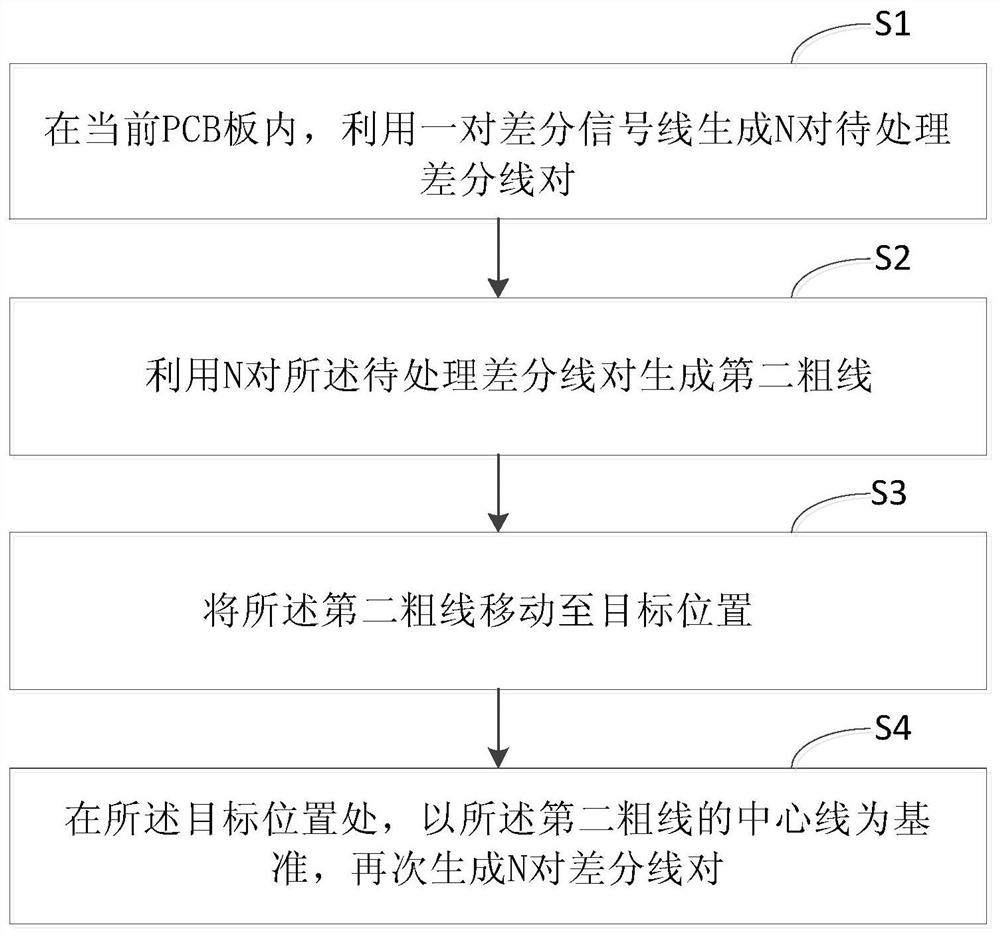
[0056] see figure 1 , figure 1 It is a schematic flowchart of a method for differential wiring in PCB design provided by the embodiment of the present application. Depend on figure 1 It can be seen that the method for differential wiring in the PCB design of this embodiment mainly includes the following processes:

[0057] S1: In the current PCB board, use a pair of differential signal lines to generate N differential line pairs to be processed.

[0058] Specifically, step S1 includes the following processes:

[0059] S11: Obtain a pair of differential values ​​of the differential line pairs to be processed in the current PCB board.

[0060] S12: Generate a pair of differential signal lines according to the differential value.

[0061] The method in this embodiment can be realized by using Cadence software. The skill language is built in the Cadence software, and the skill language can be used to program with the method in this embodiment, thereby improving the degree of ...

Embodiment 2

[0087] exist Figure 1-Figure 3 On the basis of the illustrated embodiment see Figure 4 , Figure 4 It is a schematic structural diagram of a differential wiring system in PCB design provided by the embodiment of the present application. Depend on Figure 4 It can be known that the differential wiring system in the PCB design of this embodiment mainly includes: a first wiring module, a thick line generation module, a moving module and a second wiring module.

[0088] Wherein, the first wiring module is configured to use a pair of differential signal lines to generate N differential line pairs to be processed in the current PCB board. The thick line generating module is configured to use N to-be-processed differential line pairs to generate a second thick line. A movement module for moving the second thick line to the target position. The second wiring module is configured to regenerate N pairs of differential wire pairs at the target position based on the center line of ...


PUM


Abstract

The present application discloses a method and system for differential wiring in PCB design. The method includes: using a pair of differential signal lines to generate N differential line pairs to be processed in the current PCB board; using N pairs of the differential line pairs to be processed generating a second thick line; moving the second thick line to a target position; at the target position, taking the center line of the second thick line as a reference, generating N pairs of differential line pairs again. The system includes: a first routing module, a thick line generating module, a moving module and a second routing module. Through the application, the efficiency and accuracy of differential wiring in PCB design can be effectively improved.

Description

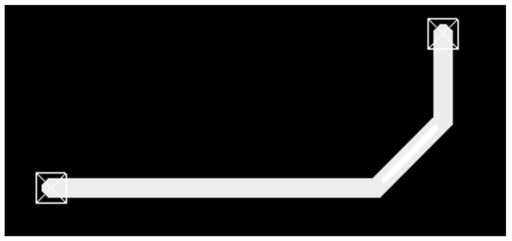
technical field [0001] The present application relates to the technical field of PCB (Printed Circuit Board, printed circuit board) design, in particular to a method and system for differential wiring in PCB design. Background technique [0002] In the PCB design and pre-evaluation stage, designers need to pre-evaluate all differential line buses, so as to continuously optimize the PCB design. With the development of high-density boards, PCB boards are becoming more and more refined and miniaturized, and the speed of differential wiring is getting higher and higher, and the requirements for the quality of differential wiring are also getting higher and higher. Therefore, how to carry out differential wiring in PCB design, so as to evaluate PCB design, is an important issue. [0003] At present, the method of differential wiring in PCB design is usually a simple evaluation. First, a thick line is drawn as the evaluation channel, and then each pair of differential signals is ...

Claims


Application Information

Patent Timeline
Patent Type & Authority Patents(China)
IPC IPC(8): H05K1/02H05K3/00
CPCH05K1/0245H05K3/0002
Inventor 吕瑞倩
Owner INSPUR SUZHOU INTELLIGENT TECH CO LTD
Learn More