Anti-EMI super junction VDMOS device

A device and conductivity type technology, applied in the field of anti-EMI superjunction VDMOS devices, can solve problems such as broadband and electromagnetic pollution, achieve current overshoot mitigation, reduce switching dv/dt and di/dt, and alleviate electromagnetic interference. Effect

Active Publication Date: 2020-06-05
UNIV OF ELECTRONICS SCI & TECH OF CHINA
View PDF12 Cites 1 Cited by
  • Summary
  • Abstract
  • Description
  • Claims
  • Application Information

AI Technical Summary

Problems solved by technology

The electromagnetic interference generated by the power VDMOS itself has a strong amplitude and a wide frequency band. These interferences will cause serious electromagnetic pollution to the surrounding components or equipment through the coupling of conduction and radiation.
Therefore, the EMI electromagnetic interference problem generated by the VDMOS device itself cannot be ignored.

Method used


Image

  • Anti-EMI super junction VDMOS device
  • Anti-EMI super junction VDMOS device
  • Anti-EMI super junction VDMOS device

Examples


Embodiment Construction

[0021] The principles and features of the present invention are described below in conjunction with the accompanying drawings, and the examples given are only used to explain the present invention, and are not intended to limit the scope of the present invention.

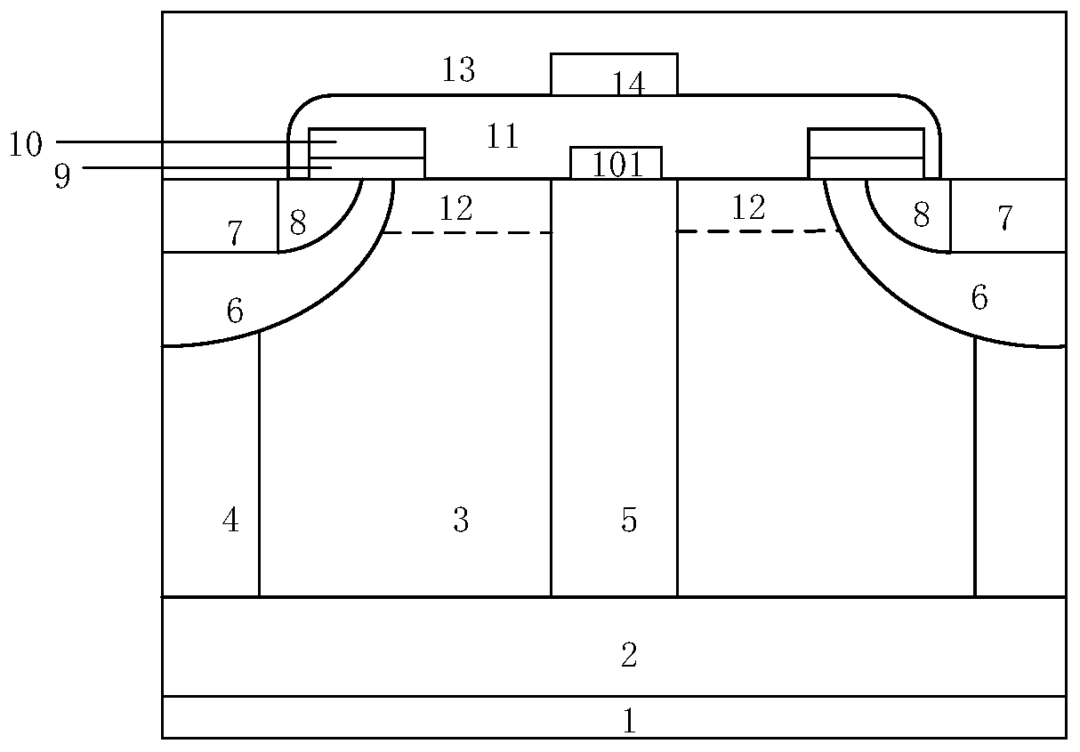
[0022] Such as figure 1 As shown, an anti-EMI super-junction VDMOS device provided by the first embodiment of the present invention includes a metallized drain 1, a heavily doped first conductivity type semiconductor substrate 2 located on the metallized drain 1, and a semiconductor substrate 2 located on the second A lightly doped first conductivity type semiconductor column 3 on a conductivity type semiconductor substrate 2; a second conductivity type located on the first conductivity type semiconductor substrate 2 and on both sides of the first conductivity type semiconductor column 3 A semiconductor column 4; a high-K dielectric material column 5 located in the first conductivity type semiconductor column 3;

...


PUM


Abstract

The invention relates to an anti-EMI super-junction VDMOS device, and belongs to the technical field of power semiconductor devices. According to the anti-EMI super-junction VDMOS device provided by the invention, a high-K dielectric material column is introduced into a drift region, and an MIS capacitor is formed by the high-K dielectric material column, a first conductive type substrate which islongitudinally adjacent to the high-K dielectric material column and a polycrystalline silicon electrode. he resistor is arranged on the dielectric layer, and the resistor is in direct contact with the metallized source electrode, so that the resistor and the MIS capacitor which are connected in series are introduced between the drain electrode and the source electrode to form an RC absorption circuit, and effective alleviation of voltage and current overshoot is realized. Therefore, the structure of the invention effectively alleviates the electromagnetic interference problem of the device on the basis of ensuring the original basic electrical properties of the super-junction VDMOS.

Description

technical field [0001] The invention belongs to the technical field of power semiconductor devices, and in particular relates to an anti-EMI super junction VDMOS device. Background technique [0002] The power super-junction VDMOS structure uses alternating P-columns and N-columns to replace the N-drift region of traditional power devices, thereby effectively reducing the on-resistance and obtaining lower on-state power consumption. Due to its unique high input impedance, low driving power, high switching speed, superior frequency characteristics, and good thermal stability, it is widely used in various fields such as switching power supplies, automotive electronics, and motor drives. [0003] The super junction VDMOS device is used as a power switch tube to control energy flow and conversion inside the system. It works in a fast switching state, and its voltage and current change sharply in a short time, resulting in a high voltage rise rate dv / dt and current rise rate di / d...

Claims


Application Information

Patent Timeline
IPC IPC(8): H01L29/78H01L29/06H01L21/336
CPCH01L29/0603H01L29/0634H01L29/0684H01L29/66712H01L29/7802
Inventor 高巍郭乔任敏李吕强蓝瑶瑶张波
Owner UNIV OF ELECTRONICS SCI & TECH OF CHINA
Why Eureka
Try Eureka