
Method for manufacturing one-time programmable device and one-time programmable device

A manufacturing method and one-off technology, applied in semiconductor/solid-state device manufacturing, electric solid-state devices, semiconductor devices, etc., can solve problems such as performance failure, easy return of metal ions, programming unit failure, etc., to achieve the effect of improving reliability

Pending Publication Date: 2020-05-29
SHANGHAI HUALI MICROELECTRONICS CORP
View PDF0 Cites 0 Cited by
  • Summary
  • Abstract
  • Description
  • Claims
  • Application Information

AI Technical Summary

Problems solved by technology

However, after the cell programming of this structure, the metal ions migrated in the high temperature process are easy to return
For one-time programmable cells based on refractory silicide, sometimes cells with smaller lengths are selected in order to reduce the size. For this structure, under high temperature conditions, serious metal return phenomenon will occur, resulting in the failure of the programmed cells, so that the entire performance fail

Method used

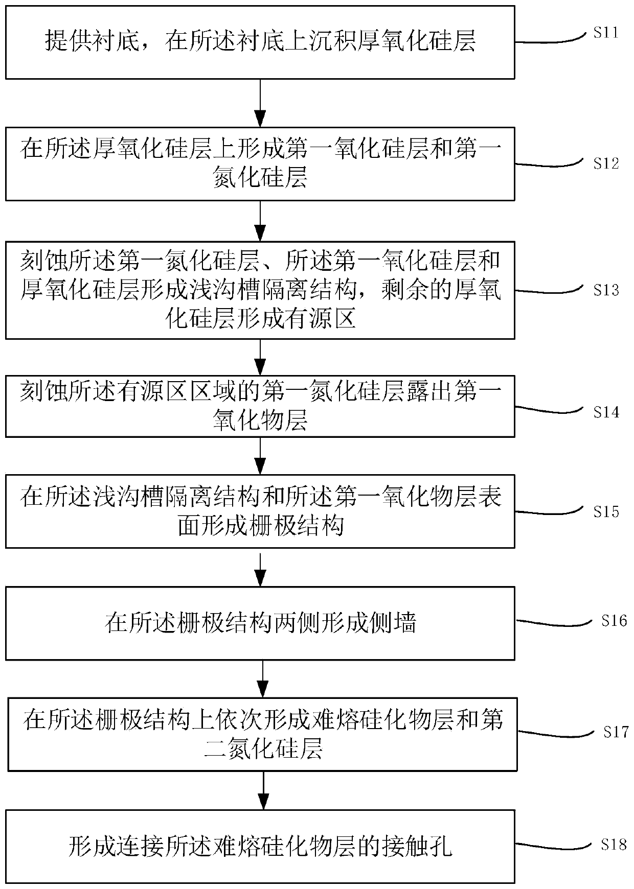
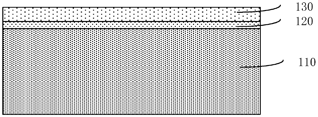

Image

  • Method for manufacturing one-time programmable device and one-time programmable device
  • Method for manufacturing one-time programmable device and one-time programmable device
  • Method for manufacturing one-time programmable device and one-time programmable device

Examples


Embodiment Construction

[0027] The specific implementation manner of the present invention will be described in more detail below with reference to schematic diagrams. The advantages and features of the present invention will be more apparent from the following description. It should be noted that all the drawings are in a very simplified form and use imprecise scales, and are only used to facilitate and clearly assist the purpose of illustrating the embodiments of the present invention.

[0028] Hereinafter, the terms "first", "second", etc. are used to distinguish between similar elements, and are not necessarily used to describe a specific order or chronological order. It is to be understood that these terms so used are interchangeable under appropriate circumstances. Similarly, if a method described herein includes a series of steps, the order in which these steps are presented is not necessarily the only order in which these steps can be performed, and some described steps may be omitted and / or...


PUM


Abstract

The invention provides a method for manufacturing a one-time programmable device and the one-time programmable device. The device comprises an active region, a shallow trench isolation structure located on one side of the active region, a first silicon oxide layer located on the active region, a gate structure located on the shallow trench isolation structure and the first silicon oxide layer, side walls located on two sides of the gate structure, a refractory silicide layer, a second silicon nitride layer, and a contact hole, wherein the refractory silicide layer and the second silicon nitride layer are sequentially located on the gate structure, and the contact hole is connected with the refractory silicide layer. A surface of the shallow trench isolation structure is higher than the surface of the first silicon oxide. A cathode end is placed in a shallow trench isolation structure region, an anode end is placed in the active region, the shallow trench isolation structure region andthe active region form a step, the refractory silicide layer also forms the step, and a grain size of the refractory silicide at the step is different from that at a plane so that migration of metal ions at the cathode end is facilitated, the migrated metal ions are not easy to return to the cathode end again, and reliability is improved.

Description

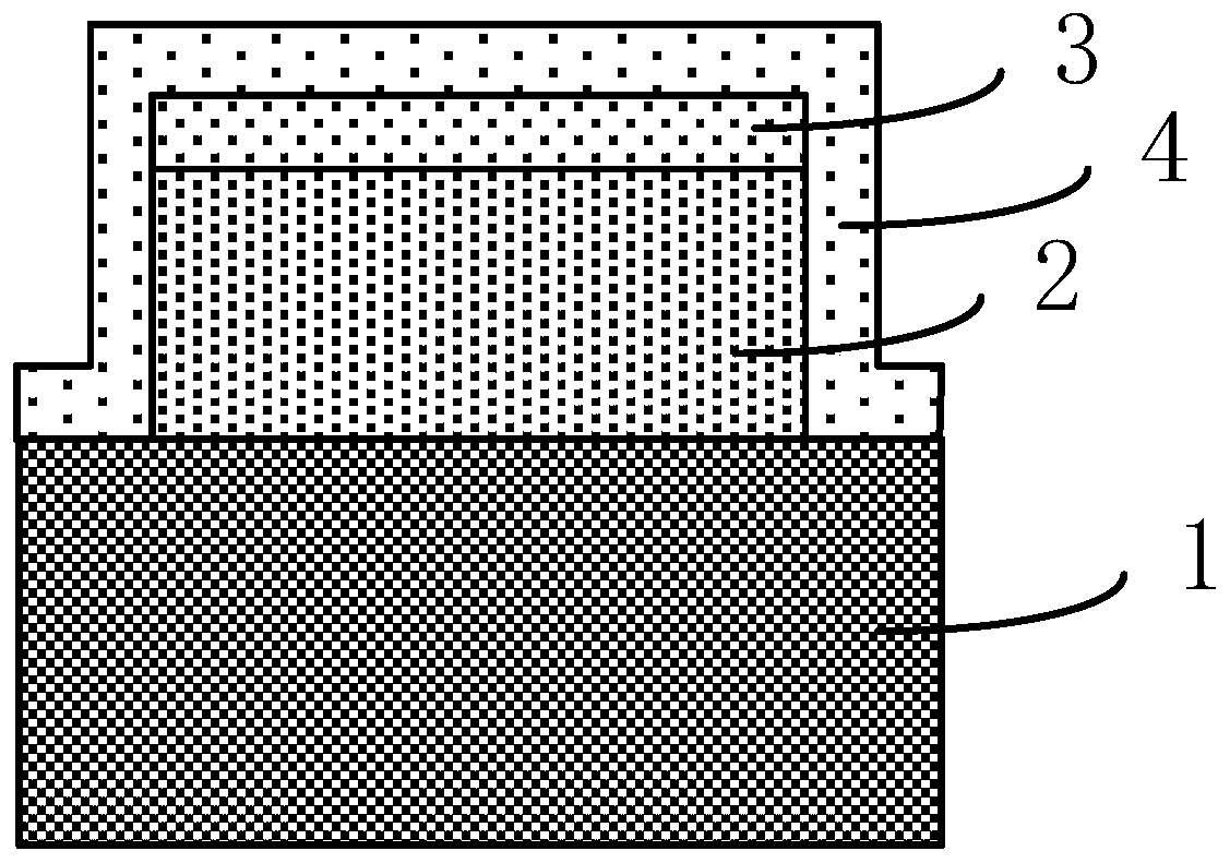
technical field [0001] The invention relates to the technical field of semiconductors, in particular to a manufacturing method of a one-time programmable device and a one-time programmable device. Background technique [0002] Compared with general-purpose and single memory, the embedded memory unit can enhance the performance of the memory, and can also reduce the area of ​​the chip. Embedded non-volatile memory is widely used in programming codes of consumer electronics, industry and automotive electronics, etc., and is widely used because the technology of the embedded memory unit is compatible with the existing technology. One type of embedded memory unit is a one-time programmable unit based on refractory silicide. Due to its good compatibility with existing processes and simple operation, it has been widely used, from 65nm logic process and 40nm logic process to 28nm The logic process is in use, and the basic structure diagram is as follows figure 1 , on the shallow ...

Claims


Application Information

Patent Timeline
IPC IPC(8): H01L27/112H01L21/8246
CPCH10B99/00H10B20/20
Inventor 田志李娟娟邵华陈昊瑜
Owner SHANGHAI HUALI MICROELECTRONICS CORP
Learn More