
PCB, manufacturing method and equipment

A PCB board and PCB connector technology, applied in the computer field, can solve the problems of increased PCB board production cost, waste of resources, increased overall thickness of PCB board, etc.

Active Publication Date: 2020-05-26
ZTE CORP
View PDF6 Cites 0 Cited by
  • Summary
  • Abstract
  • Description
  • Claims
  • Application Information

AI Technical Summary

Problems solved by technology

[0005] The purpose of the embodiment of the present invention is to provide a PCB board, manufacturing method and equipment to solve the problems in the prior art due to the need to add additional signal layers to transmit high-speed signals The resulting increase in the overall thickness of the PCB board leads to an increase in the production cost of the PCB board, resulting in a technical problem of waste of resources

Method used


Image

  • PCB, manufacturing method and equipment
  • PCB, manufacturing method and equipment
  • PCB, manufacturing method and equipment

Examples


Embodiment Construction

[0023] In order to make the purpose, technical solution and advantages of the present application clearer, the technical solution of the present application will be clearly and completely described below in conjunction with specific embodiments of the present application and corresponding drawings. Apparently, the described embodiments are only some of the embodiments of the present application, rather than all the embodiments. Based on the embodiments in this application, all other embodiments obtained by persons of ordinary skill in the art without making creative efforts belong to the scope of protection of this application.

[0024] The technical solutions provided by various embodiments of the present application will be described in detail below in conjunction with the accompanying drawings.

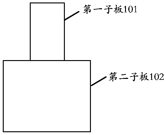
[0025] See figure 2 , a structural schematic diagram of the PCB board provided by the embodiment of the present invention, such as figure 2 As shown, the PCB board may include:...


PUM


Abstract

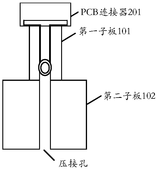
The invention discloses a PCB, a manufacturing method and equipment. The PCB at least comprises a first daughter board and a second daughter board, wherein the first daughter board is located on the second daughter board, the size of the first daughter board is smaller than that of the second daughter board, and the first daughter board is connected with a PCB connector. In the invention, the second daughter board can be connected with the PCB connector through the first daughter board, so that the second daughter board is not directly connected with the PCB connector, and all signal layers ofthe second daughter board can transmit high-speed signals; correspondingly, the second daughter board does not need to additionally add a signal layer, so that compared with a PCB in the prior art, the number of signal layers of the second daughter board is smaller; and correspondingly, the thickness of the second daughter board is smaller. Although the second daughter board needs to be connectedwith the first daughter board, the size of the first daughter board is smaller than that of the second daughter board, so that only the local thickness is increased, and the overall thickness is notincreased. Therefore, the overall thickness of the PCB is not increased due to connection with the PCB connector, the manufacturing cost is effectively reduced, and resource waste is reduced.

Description

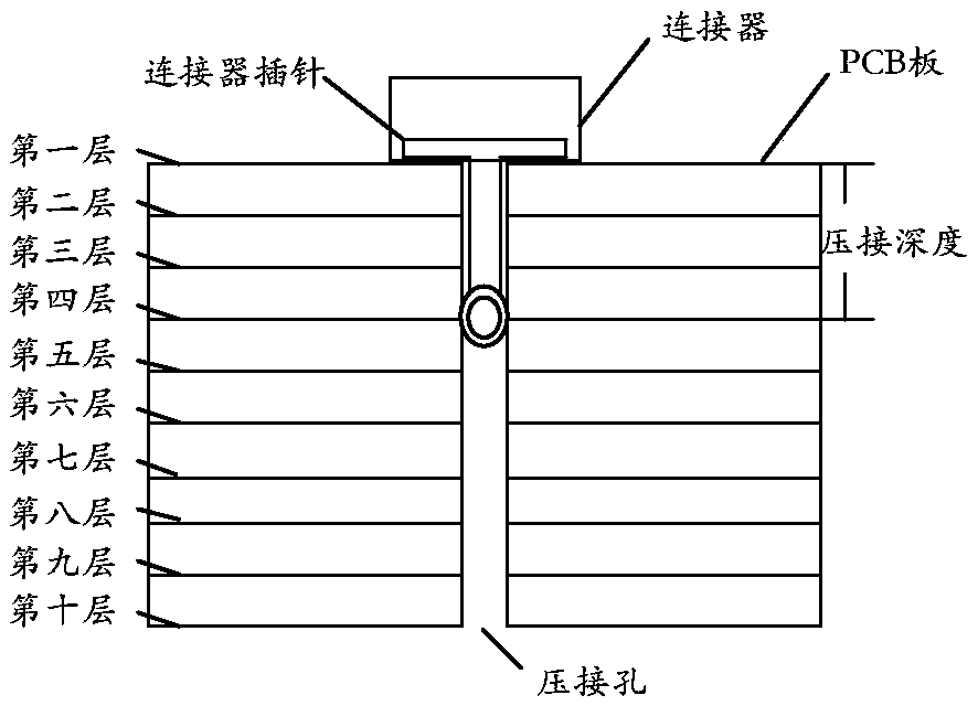
technical field [0001] The present application relates to the field of computer technology, and in particular to a PCB (Printed Circuit Board, printed circuit board) board, manufacturing method and equipment. Background technique [0002] In the prior art, the connector can be deployed on the PCB board by means of crimping, specifically, as figure 1 As shown, the pins on the connector can be pressed into the crimping holes on the PCB to realize the crimping of the connector and the PCB. [0003] When crimping the PCB board and the connector, in order to ensure the reliability of the crimping, when back drilling the crimping hole, the crimping depth (that is, the depth of the pins on the connector pressed into the PCB board during crimping) cannot be adjusted. ) inside the crimp hole (such as figure 1 Corresponding crimp holes for layers 1 through 4 shown) are backdrilled. And when the crimp hole outside the crimp depth (such as figure 1 When the crimping holes correspond...

Claims


Application Information

Patent Timeline
IPC IPC(8): H05K1/02H05K1/14H05K1/18H05K3/30
CPCH05K1/02H05K1/14H05K1/18H05K3/30
Inventor 尹昌刚曹化章王迎新
Owner ZTE CORP
Learn More