Surface acoustic wave filter packaging structure and manufacturing method thereof

A packaging structure, surface acoustic wave technology, applied in electrical components, impedance networks, etc., can solve problems such as failure to improve, simplify the production process, and damage

Active Publication Date: 2020-05-19
PHOENIX PIONEER TECH
View PDF7 Cites 5 Cited by
  • Summary
  • Abstract
  • Description
  • Claims
  • Application Information

AI Technical Summary

Problems solved by technology

[0006] However, in the design of the electrical connection of the existing surface acoustic wave filter packaging structure of the wafer level package, the upper chip 15 and the lower chip 11 are first connected and bonded, and then the electroplating process is used to form an electroplated metal outside the package structure. thin film 16, which not only fails to simplify the manufacturing process, but also easily contaminates or damages the chip in the related process, resulting in the failure to improve the yield control and cost control of the process.

Method used


Image

  • Surface acoustic wave filter packaging structure and manufacturing method thereof
  • Surface acoustic wave filter packaging structure and manufacturing method thereof
  • Surface acoustic wave filter packaging structure and manufacturing method thereof

Examples


Embodiment Construction

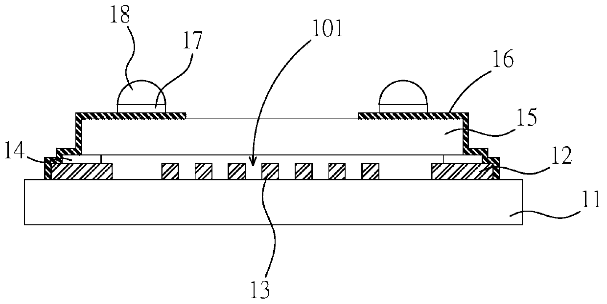
[0057] The advantages and spirit of the present invention can be further understood through the following detailed description of the invention and the accompanying drawings. The manufacture and use of the preferred embodiment of the present invention are described in detail as follows. It must be understood that the present invention provides many applicable innovative concepts that can be broadly implemented within a particular background. This specific embodiment is only shown in a specific way to make and use the invention, but does not limit the scope of the invention.

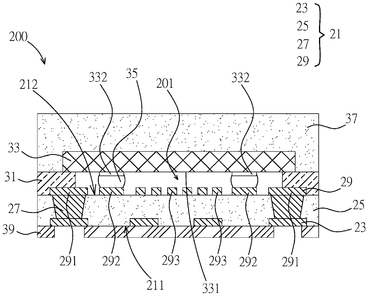
[0058] Please refer to the figure, the surface acoustic wave filter package structure 200 according to the preferred embodiment of the present invention includes a dielectric substrate 21, a chip 33, a polymer sealing frame 31, a molding layer 37 and a patterned protective layer 39 .

[0059] The dielectric substrate 21 has a dielectric layer 25 , a first patterned conductive layer 23 , a second pattern...


PUM

PropertyMeasurementUnit
thicknessaaaaaaaaaa

Abstract

The invention discloses a surface acoustic wave filter packaging structure. The structure comprises a dielectric substrate, wherein the substrate comprises a dielectric layer, a first patterned conductive layer, a second patterned conductive layer and a conductive connecting layer, the conductive connecting layer is arranged in the dielectric layer and electrically connected with the first patterned conductive layer and the second patterned conductive layer which are arranged on the two sides of the dielectric layer respectively and the second patterned conductive layer is at least provided with an interdigital electrode part, a chip, wherein the active surface of the chip is opposite to the interdigital electrode part, a polymer sealing frame body which is arranged between the chip and the dielectric substrate and is arranged at the periphery of the chip in a surrounding manner, so that the polymer sealing frame body, the chip and the dielectric substrate form a closed cavity together, and a mold sealing layer which is arranged on the dielectric substrate and covers the chip and the polymer sealing frame body. The invention further provides a manufacturing method of the surface acoustic wave filter packaging structure.

Description

technical field [0001] The present invention relates to a semiconductor package and its manufacturing method, and in particular to a surface acoustic wave filter packaging structure and its manufacturing method. Background technique [0002] Surface acoustic wave filter (Surface Acoustic Wave filter, SAW filter) is a common component in communication systems. Its operating principle is to convert the received electrical signal into mechanical waves in piezoelectric materials. Due to the delay in the transmission of mechanical waves through piezoelectric materials , and then through the output electrode to convert the delayed mechanical wave into electrical energy signal. By combining the delayed output signal to reproduce the result, the goal of filtering unnecessary signals and noise and improving the quality of receiving can be achieved. [0003] At the same time, due to the design flexibility of the surface acoustic wave filter, analog / digital compatibility, excellent gr...

Claims


Application Information

Patent Timeline
Patent Type & Authority Applications(China)
IPC IPC(8): H03H9/02H03H9/10H03H9/145H03H9/64
CPCH03H9/02574H03H9/02818H03H9/1064H03H9/145H03H9/64
Inventor 许诗滨许哲玮
Owner PHOENIX PIONEER TECH
Why Eureka
Try Eureka