Wave absorbing/transmitting device of composite window absorber
An absorber and wave-transmitting technology, which can be applied to antennas, electrical components, etc., can solve the problem of difficulty in taking into account at the same time, and achieve the effects of easy assembly, low cost, and wide absorbing frequency.
- Summary
- Abstract
- Description
- Claims
- Application Information
AI Technical Summary
Problems solved by technology
Method used
Image
Examples
Embodiment 1
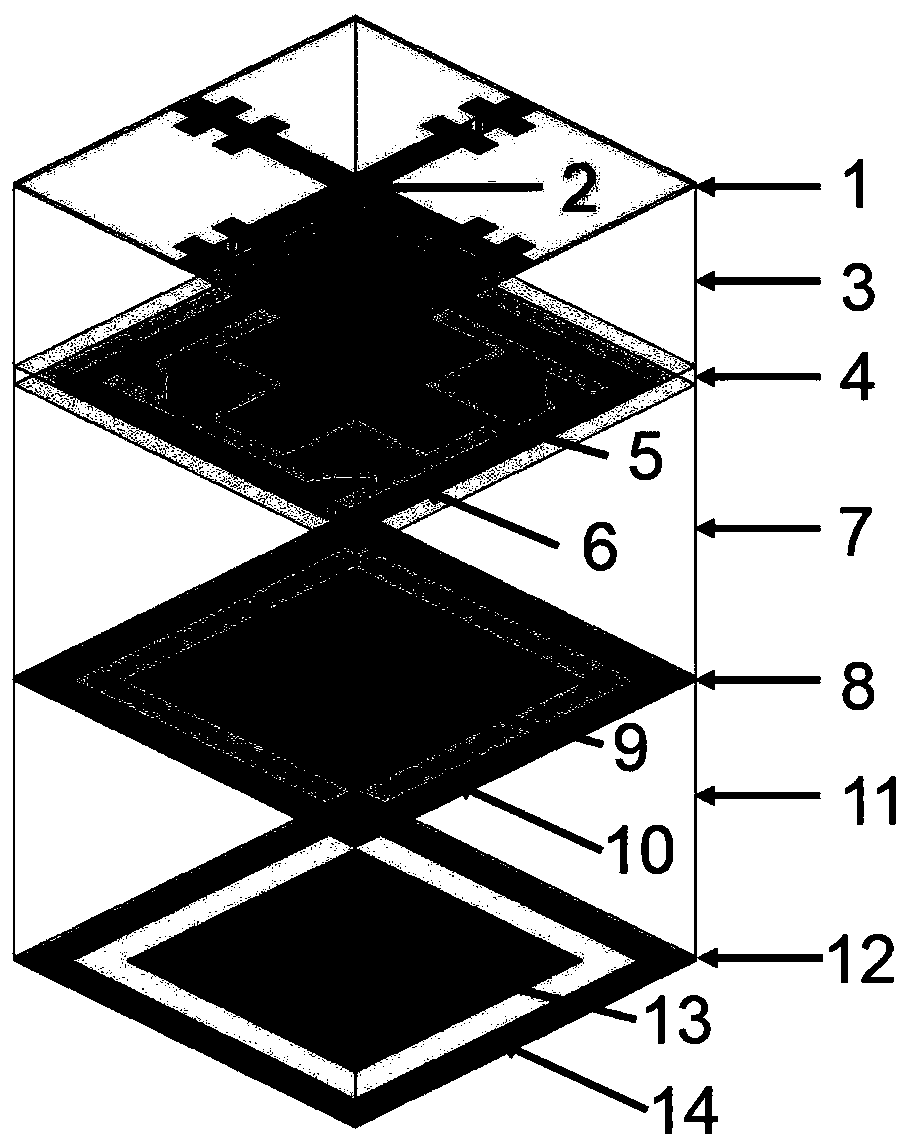
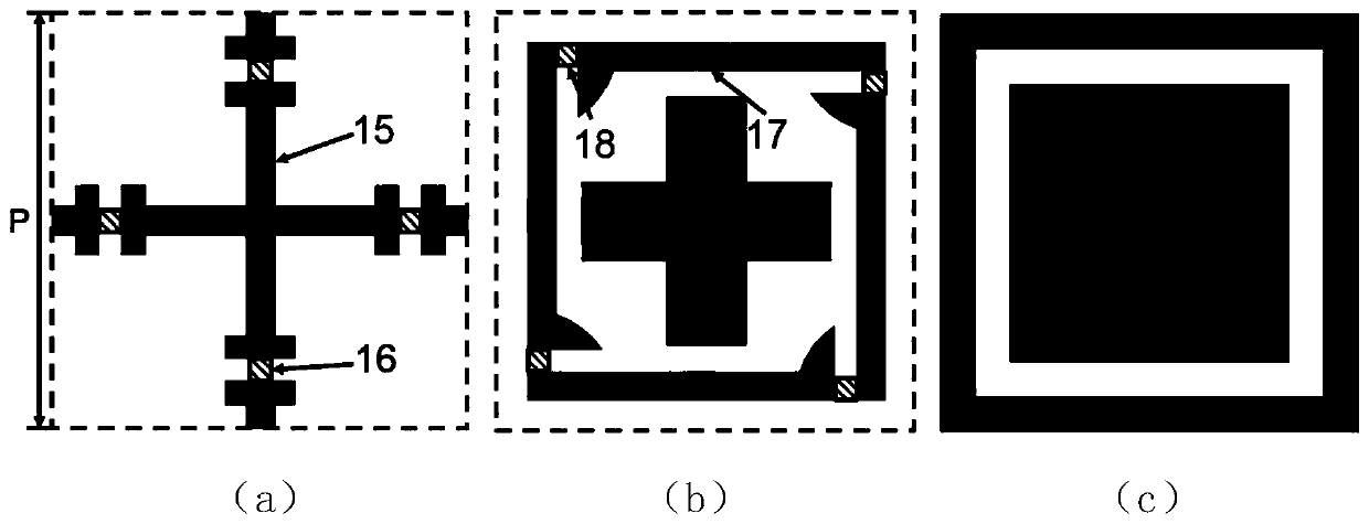
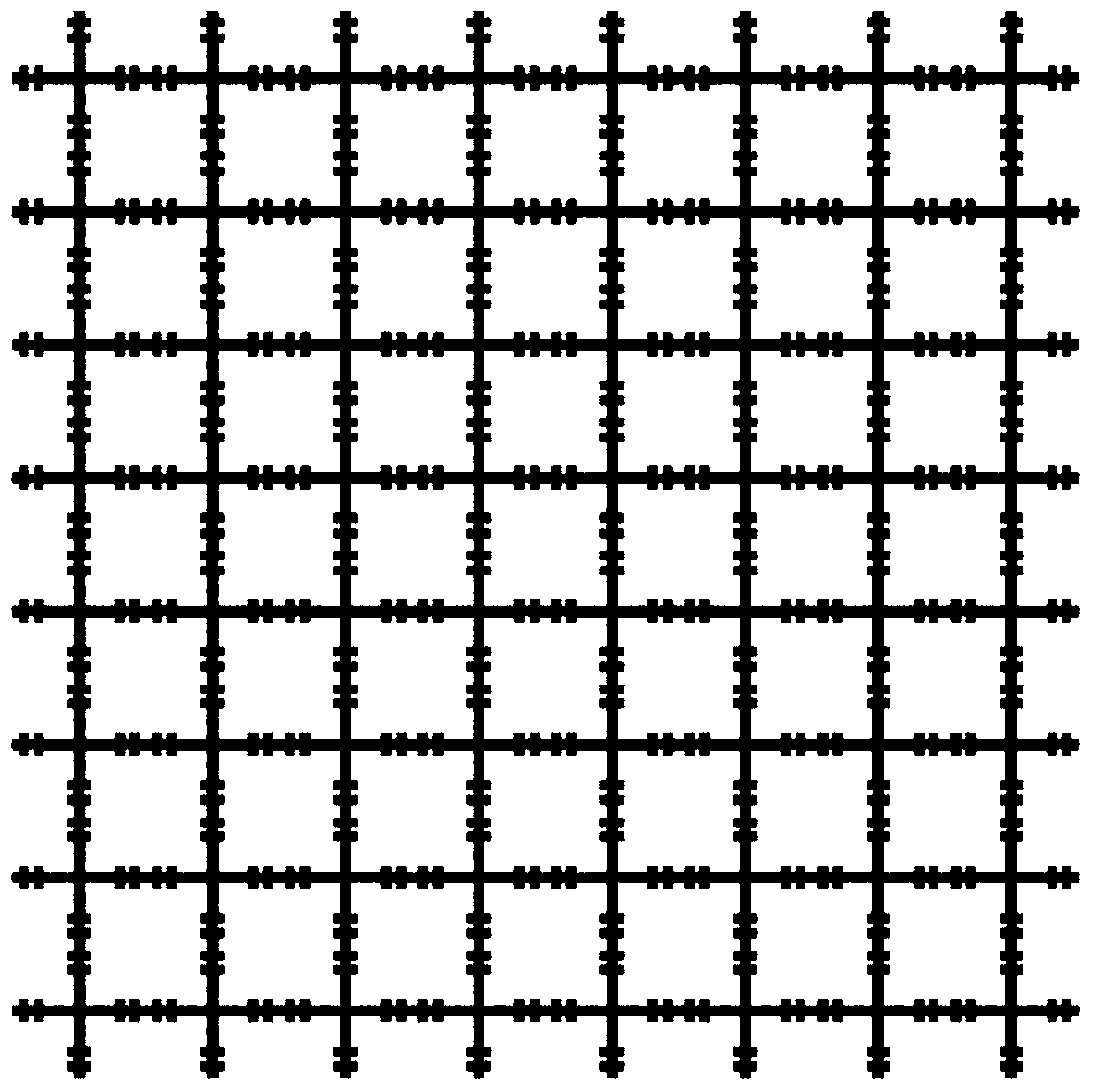
[0055]The first wave-absorbing layer 1 is a single-sided copper-clad board. The copper foil is processed with cross-shaped patterns 2 periodically arranged in rows and columns. The width of the cross structure is 1.25 mm. Each cross-shaped pattern 2 is provided with eight slits. Wherein the gap length of welding lumped resistor 15 is 1.5mm, the gap length of welding lumped inductance 16 is 1.0mm, the resistance value of any one lumped resistor 15 is 50ohm, the inductance value of any one lumped inductor 16 is 10nH, ten The FSS unit period of the first layer of wave-absorbing layer composed of zigzag pattern 2, lumped resistance 15 and inductance 16 is 18mm; the first dielectric isolation layer 3 is made of aramid paper honeycomb material with a thickness of 8.5mm, and its relative permittivity is 1.07, and the dielectric loss tangent is 0.0017. The second wave-absorbing layer 4 is a single-sided copper-clad board. The copper foil is processed with cross patch patterns 5 and op...
Embodiment 2
[0058] The first wave-absorbing layer 1 is a single-sided copper-clad board, and the copper foil is processed with cross-shaped patterns 2 periodically arranged in rows and columns. The width of the cross-shaped structure is 2 mm, and each cross-shaped pattern 2 is provided with eight slits. The gap length of welding lumped resistor 15 is 1.5mm, the gap length of welding lumped inductance 16 is 1.0mm, the resistance value of any one lumped resistor 15 is 50ohm, the inductance value of any one lumped inductor 16 is 8nH, cross-shaped Pattern 2, lumped resistance 15 and inductance 16 form the first wave-absorbing layer FSS unit period is 20mm; the first dielectric isolation layer 3 is made of aramid paper honeycomb material with a thickness of 8.5mm, and its relative permittivity is 1.07, and the dielectric loss tangent is 0.0017. The second wave-absorbing layer 4 is a single-sided copper-clad board. The copper foil is processed with cross patch patterns 5 and open square ring pa...
PUM
| Property | Measurement | Unit |
|---|---|---|
| Thickness | aaaaa | aaaaa |
| Thickness | aaaaa | aaaaa |
| Line width | aaaaa | aaaaa |
Abstract
Description
Claims
Application Information
 - R&D
- Intellectual Property
- Life Sciences
- Materials
- Tech Scout
- Unparalleled Data Quality
- Higher Quality Content
- 60% Fewer Hallucinations
Browse by: Latest US Patents, China's latest patents, Technical Efficacy Thesaurus, Application Domain, Technology Topic, Popular Technical Reports.
© 2025 PatSnap. All rights reserved.Legal|Privacy policy|Modern Slavery Act Transparency Statement|Sitemap|About US| Contact US: help@patsnap.com


