
Cleaning frame applied to solar silicon wafer

A technology for solar silicon wafers and cleaning racks, which is applied in the directions of cleaning methods using liquids, cleaning methods and utensils, sustainable manufacturing/processing, etc., which can solve the problem of low cleaning degree of silicon wafers, affecting the use of silicon wafers, and poor fixing effect of silicon wafers and other problems, to achieve the effect of enhanced cleaning effect, simple structure and convenient operation.

Inactive Publication Date: 2020-05-12
合肥敬卫新能源有限公司
View PDF0 Cites 0 Cited by
  • Summary
  • Abstract
  • Description
  • Claims
  • Application Information

AI Technical Summary

Problems solved by technology

[0003] The technical problem to be solved by the present invention is that the traditional cleaning rack for silicon wafers has a poor effect of fixing silicon wafers, and the degree of cleanliness of silicon wafers is low, which affects the use of silicon wafers. A cleaning rack for solar silicon wafers is now provided

Method used


Image

  • Cleaning frame applied to solar silicon wafer
  • Cleaning frame applied to solar silicon wafer
  • Cleaning frame applied to solar silicon wafer

Examples


Embodiment

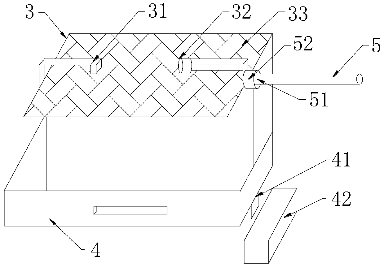
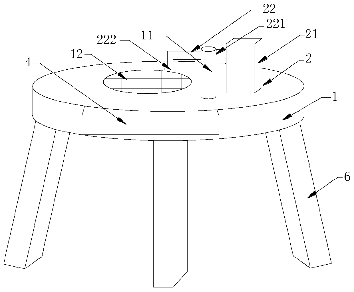
[0021] Example: such as Figure 1-2 As shown, a cleaning rack applied to solar silicon wafers includes a working platform 1, a cleaning assembly 2 positioned at the working platform 1, and a fixed frame 3 arranged inside the working platform 1; the working platform 1 includes a spray gun bar 11, a spraying Area 12; the spray gun bar 11 is arranged on the surface of the working platform 1, the spray area 12 is located at one side of the spray gun bar 11, and the spray area 12 is composed of several spray through holes, and the cleaning assembly 2 includes a water tank 21 and a spray gun 22; The water tank 21 is located on the surface of the working platform 1 and is on the same horizontal line as the spray gun rod 11. The spray gun 22 is located on the top of the spray gun rod 11. The spray gun 22 is on the same vertical line as the spraying area 12 on the surface of the working platform 1. The bottom of the spray gun 22 passes The water pipe is fixedly connected to the water t...


PUM


Abstract

The invention discloses a cleaning frame applied to a solar silicon wafer. The cleaning frame comprises a working platform, a cleaning assembly located on the working platform and a fixing frame arranged inside the working platform; the working platform comprises a spray gun rod and a spraying area; the spray gun rod is arranged on the surface of the working platform, the spraying area is arrangedon one side of the spray gun rod, and the cleaning assembly comprises a water tank and a spray gun; the water tank is located on the surface of the working platform and located on the same horizontalline with the spray gun rod, the spray gun is located at the top end of the spray gun rod, the bottom end of the spray gun is fixedly connected with the water tank through a water pipe, the working platform is internally provided with a cleaning drawer, and the fixing frame comprises a fixing clamp buckle, a clamp ring and a cleaning net; and the cleaning net is arranged inside the cleaning drawer, the two ends of the cleaning net are connected with the cleaning drawer through fixing rods arranged on the two sides of the cleaning net, the fixing clamp buckle is located on one side of the cleaning net, and the clamp ring is arranged at the position, corresponding to the fixing clamp buckle, of the other side of the cleaning net and movably connected with the fixing clamp buckle.

Description

technical field [0001] The invention relates to the technical field of silicon wafer cleaning devices, in particular to a cleaning rack applied to solar silicon wafers. Background technique [0002] With the development of large-scale integrated circuits, the continuous improvement of integration and the continuous reduction of line width, the quality requirements of silicon wafers are getting higher and higher, especially the surface quality requirements of silicon wafers are becoming stricter and stricter. This is mainly because the particles and metal impurities on the polished surface of the silicon wafer will seriously affect the quality and yield of the device. In the current production of integrated circuits, if silicon wafers are not cleaned thoroughly, all silicon wafers may be scrapped, or the manufactured devices have poor performance, poor stability and reliability. For the existing cleaning racks, due to unreasonable design, the cleaning rack has a poor fixing ...

Claims


Application Information

Patent Timeline
Patent Type & Authority Applications(China)
IPC IPC(8): B08B3/02B08B13/00H01L31/18
CPCB08B3/022B08B13/00H01L31/18Y02P70/50
Inventor 程林
Owner 合肥敬卫新能源有限公司
Learn More