A packaging method for densely arranging semiconductor chips for Internet of Things terminals

An IoT terminal and packaging method technology, which is applied to semiconductor devices, semiconductor/solid-state device components, and electric solid-state devices, etc., can solve the problems of chip pulling, chip damage, and easy torn chips at the connection between the chip and the pin. , to achieve the effect of good fixing effect and simple structure

Active Publication Date: 2022-04-29
袁晓华
View PDF5 Cites 0 Cited by
  • Summary
  • Abstract
  • Description
  • Claims
  • Application Information

AI Technical Summary

Problems solved by technology

[0003] At present, there are many ways to package semiconductor chips, but they are similar. Most of the connection methods between the chip and the pins are directly connected. Since the pins are extended to the outside of the package, the pins will be accidentally pulled during installation or transportation. pins, it is easy to tear the chip inside the package, and the connection between the chip and the pin is also easy to be torn off. In addition, when the chip is finally plastic-packed, the plastic shell must press the chip. If the control is not good, it is easy to cause damage to the chip.

Method used


Image

  • A packaging method for densely arranging semiconductor chips for Internet of Things terminals
  • A packaging method for densely arranging semiconductor chips for Internet of Things terminals
  • A packaging method for densely arranging semiconductor chips for Internet of Things terminals

Examples


Embodiment 1

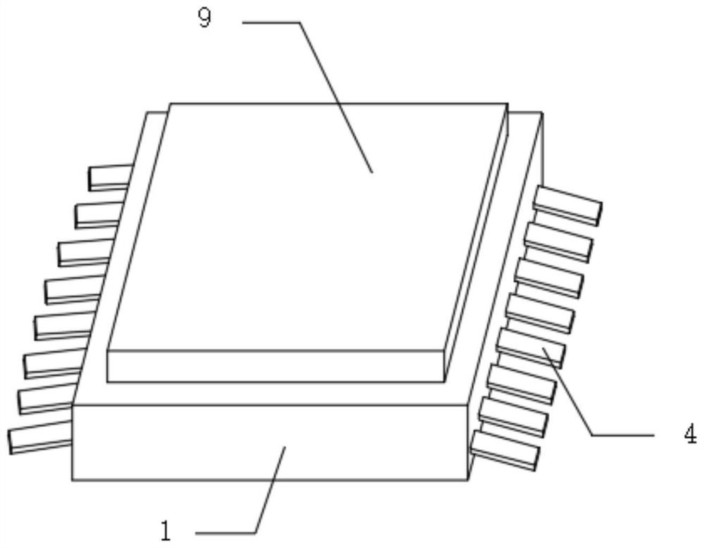
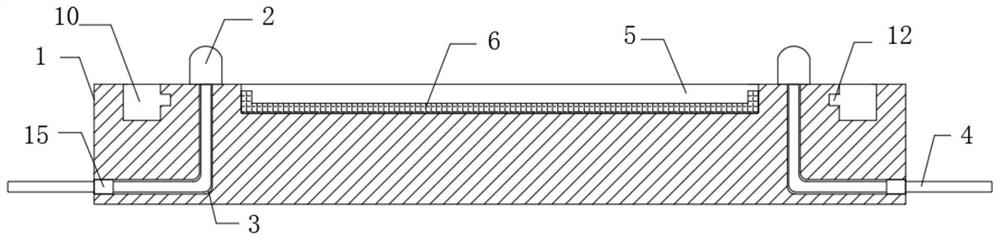
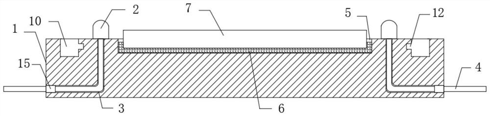
[0044] see Figure 1-7 , a packaging method for densely arranging semiconductor chips for Internet of Things terminals, including a lower housing 1, see figure 1 , the upper surface of the lower casing 1 is provided with a placement groove 5, and the upper surface of the lower casing 1 is fixedly connected with two sets of conductive columns 2, and the two sets of conductive columns 2 are respectively located on both sides of the placement groove 5, and the lower casing 1 There is a perforation 3 inside, the shape of the perforation 3 is L-shaped, and the lower opening of the perforation 3 is filled with insulating glue 15, because there is a corner on the L-shaped perforation 3, so that when the leaked pin 4 is involved At this time, the hole wall at the corner can play a counterweight role to prevent the conductive column 2 from being affected, the insulating glue 15 plays the role of insulation, and also plays the role of sealing, and the perforation 3 is located below the ...


PUM


Abstract

The invention discloses a packaging method for densely arranging semiconductor chips for an Internet of Things terminal, belonging to the field of semiconductor packaging, and a packaging method for densely arranging semiconductor chips for an Internet of Things terminal, including the upper surface of a lower casing There is a placement slot, and two sets of conductive columns are fixedly connected to the upper surface of the lower case, and the two sets of conductive posts are respectively located on both sides of the placement slot, and there are perforations in the lower case, and the perforations are located below the conductive posts. Pins are placed in the center, and the upper ends of the pins are fixedly connected with the conductive columns, the bottom of the placement groove is bonded with adhesive, the chip is placed in the placement groove, and the lower end of the chip is bonded with the adhesive, the upper surface of the chip is It can realize the indirect connection between the chip and the pins by connecting multiple wires to the conductive posts, so as to prevent the pins from being involved in the chip and causing the chip to shake or be damaged. effect without damaging the chip.

Description

technical field [0001] The present invention relates to the field of semiconductor packaging, and more specifically, to a packaging method for densely arranging semiconductor chips used in Internet of Things terminals. Background technique [0002] Packaging technology is necessary and crucial for the chip, because the chip must be isolated from the outside world to prevent impurities in the air from corroding the chip circuit and causing electrical performance degradation. On the other hand, the packaged chip is also more It is convenient for installation and transportation, because the packaging technology directly affects the performance of the chip itself and the design and manufacture of the PCB connected to it, so it is very important. [0003] At present, there are many ways to package semiconductor chips, but they are similar. Most of the connection methods between the chip and the pins are directly connected. Since the pins are extended to the outside of the package...

Claims


Application Information

Patent Timeline
Patent Type & Authority Patents(China)
IPC IPC(8): H01L23/055H01L23/24H01L23/48
CPCH01L23/055H01L23/24H01L23/48
Inventor 袁晓华
Owner 袁晓华
Why Eureka
Try Eureka