Electromagnetic interference time domain analysis method of microstrip line on electromagnetic wave effect PCB

An electromagnetic interference and time-domain analysis technology, applied in the fields of electrical digital data processing, CAD circuit design, special data processing applications, etc., can solve problems such as consuming large computing resources, avoid direct modeling, and improve computing efficiency.

Pending Publication Date: 2020-04-28
CHONGQING UNIV OF POSTS & TELECOMM
View PDF12 Cites 1 Cited by
  • Summary
  • Abstract
  • Description
  • Claims
  • Application Information

AI Technical Summary

Problems solved by technology

[0004] The technical problem to be solved by the present invention is to provide an efficient time-domain hybrid algorithm to quickly simulate and analyze the electromagnetic interference caused by electromagnetic waves on the microstrip line in view of the shortcomings of the prior art that consume a large amount of computing resources when dealing with the electromagnetic interference of the microstrip line. interference problem

Method used


Image

  • Electromagnetic interference time domain analysis method of microstrip line on electromagnetic wave effect PCB
  • Electromagnetic interference time domain analysis method of microstrip line on electromagnetic wave effect PCB
  • Electromagnetic interference time domain analysis method of microstrip line on electromagnetic wave effect PCB

Examples


Embodiment Construction

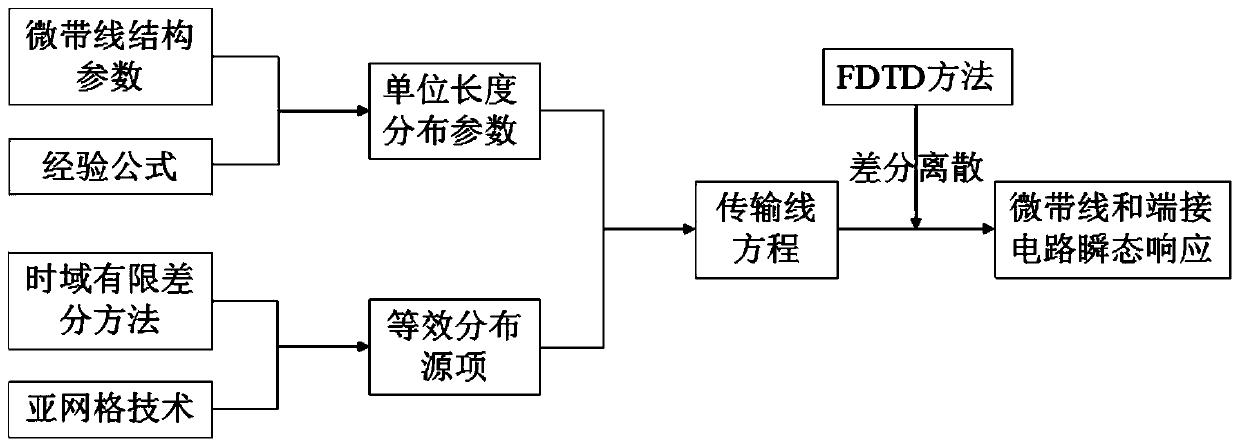
[0020] The technical solution of the present invention will be described in detail below in conjunction with the accompanying drawings and embodiments.

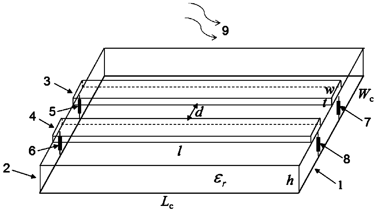
[0021] In this embodiment, the electromagnetic interference caused by electromagnetic waves acting on two microstrip lines is taken as an example for illustration.

[0022] The electromagnetic coupling model of electromagnetic waves acting on two microstrip lines is as follows: figure 2 As shown, it includes ground plate 1, substrate 2, microstrip lines 3, 4, loads 5, 6, 7, 8, and electromagnetic wave 9. The dimension of the ground plate 1 is L c ×W c . The thickness of the substrate 2 is h, and the relative permittivity of the selected material is ε r . The microstrip line 3 and the microstrip line 4 are rectangular metal strips, the length of which is l, the cross-sectional width is w, and the thickness is t. Load 5, load 6, load 7 and load 8 are resistors, and the resistance value of the resistors can be defined by ...


PUM


Abstract

The invention provides an electromagnetic interference time domain analysis method for a microstrip line on an electromagnetic wave effect PCB, and the method comprises the steps: firstly building anelectromagnetic coupling model of a microstrip line on an electromagnetic wave effect PCB by employing a transmission line equation, wherein the modeling precision of the transmission line equation depends on unit length distribution parameters and equivalent distribution source items of the microstrip line; therefore, according to the structural size of the microstrip line, the unit length distribution parameters of the microstrip line are calculated in combination with an empirical formula. Then, modeling of a substrate and a grounding plate of the PCB is conducted by adopting a time domainfinite difference (FDTD) method in combination with a sub-grid technology, an excitation field of the microstrip line is obtained through calculation, and the excitation field is introduced into a transmission line equation to serve as an equivalent distribution source item; and after a transmission line equation is established, discretization is carried out by adopting a central difference formatof an FDTD method, so that the transient response on the microstrip line and a terminating circuit is obtained through iterative solution. According to the method, direct modeling of a microstrip line structure is avoided, and the problem that the calculation efficiency is low due to the fact that the grid amount needed by subdivision is large when microstrip line electromagnetic coupling on thePCB is simulated through a traditional full-wave algorithm can be effectively solved.

Description

technical field [0001] The invention relates to an electromagnetic interference analysis method of a microstrip line on a PCB, and proposes an efficient time-domain mixing algorithm, which is suitable for fast simulation and analysis of electromagnetic interference of an electromagnetic wave on a microstrip line. Background technique [0002] With the rapid development of 4G and 5G communication technologies, the integration of electronic equipment used in communication, electronics and other fields is getting higher and higher. Circuits in electronic equipment integrate semiconductor devices and microwave and millimeter wave chips into PCB boards, and data transmission and communication are performed between devices and chips through microstrip lines. For the PCB board circuit, the power that can be tolerated is relatively small. Under the action of a strong electromagnetic radiation source in space, electromagnetic interference signals will be generated through microstrip ...

Claims


Application Information

Patent Timeline
IPC IPC(8): G06F30/3308G06F30/367G06F115/12
CPCY02E60/00
Inventor 叶志红吴小林周健健苟丹石艳超汝梦祖
Owner CHONGQING UNIV OF POSTS & TELECOMM
Why Eureka
Try Eureka