Indium bump resetting method for infrared detector reading circuit
A technology of infrared detectors and readout circuits, applied in circuits, electrical components, semiconductor devices, etc., can solve problems such as waste
- Summary
- Abstract
- Description
- Claims
- Application Information
AI Technical Summary
Problems solved by technology
Method used
Image
Examples
Embodiment Construction
[0033] Exemplary embodiments of the present disclosure will be described in more detail below with reference to the accompanying drawings. Although exemplary embodiments of the present disclosure are shown in the drawings, it should be understood that the present disclosure may be embodied in various forms and should not be limited by the embodiments set forth herein. Rather, these embodiments are provided for more thorough understanding of the present disclosure and to fully convey the scope of the present disclosure to those skilled in the art.
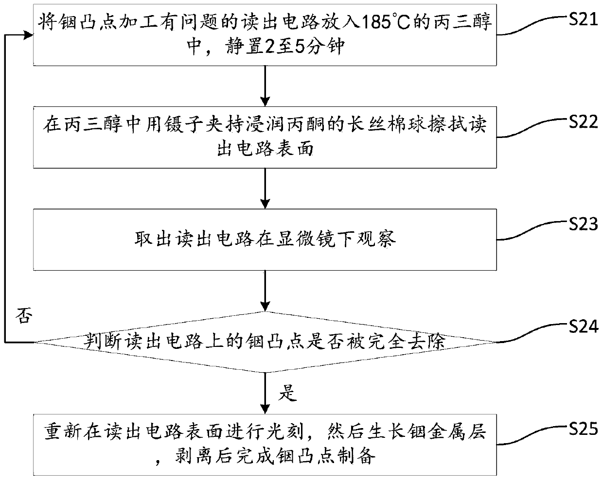
[0034] The embodiment of the present invention proposes a method for resetting the indium bump of the infrared detector readout circuit, such as figure 1 As shown, the method includes:
[0035] S11, immersing the readout circuit in glycerin with a preset temperature T and standing still, so as to remove scrapped indium bumps on the readout circuit;
[0036] S12, resetting standard indium bumps on the readout circuit from which sc...
PUM
| Property | Measurement | Unit |
|---|---|---|
| melting point | aaaaa | aaaaa |
Abstract
Description
Claims
Application Information
 - R&D
- Intellectual Property
- Life Sciences
- Materials
- Tech Scout
- Unparalleled Data Quality
- Higher Quality Content
- 60% Fewer Hallucinations
Browse by: Latest US Patents, China's latest patents, Technical Efficacy Thesaurus, Application Domain, Technology Topic, Popular Technical Reports.
© 2025 PatSnap. All rights reserved.Legal|Privacy policy|Modern Slavery Act Transparency Statement|Sitemap|About US| Contact US: help@patsnap.com


