
Display panel and display device

A display panel and display area technology, which is applied in the direction of diodes, semiconductor devices, electrical components, etc., can solve the problems that the optical and electronic components 100 cannot receive sufficient light, and the image quality of the optical and electronic components 100 is reduced, so as to improve the transmittance, The effect of improving image quality

Active Publication Date: 2020-02-04
WUHAN TIANMA MICRO ELECTRONICS CO LTD
View PDF9 Cites 2 Cited by
  • Summary
  • Abstract
  • Description
  • Claims
  • Application Information

AI Technical Summary

Problems solved by technology

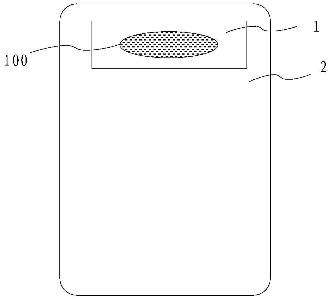
[0004] However, due to the strong reflection of the light by the thin silver layer in the region 1, the optical electronic element 100 cannot receive sufficient light, thereby reducing the imaging quality of the optical electronic element 100

Method used


Image

  • Display panel and display device
  • Display panel and display device
  • Display panel and display device

Examples


Embodiment Construction

[0051] "First" and "second" in the description and claims of the present invention and the above drawings are used to distinguish different objects, rather than to describe a specific order. Furthermore, the term "comprise", as well as any variations thereof, are intended to cover a non-exclusive inclusion. For example, a process, method, system, product or device comprising a series of steps or units is not limited to the listed steps or units, but optionally also includes unlisted steps or units, or optionally further includes For other steps or units inherent in these processes, methods, products or apparatuses.

[0052] The term "and / or" in this article is just an association relationship describing associated objects, which means that there can be three relationships, for example, A and / or B can mean: A exists alone, A and B exist simultaneously, and there exists alone B these three situations. In addition, the character " / " in this article, unless otherwise specified, ...


PUM


Abstract

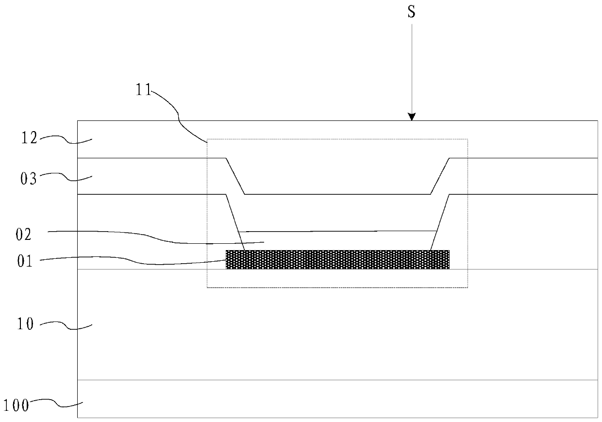
The invention provides a display panel and a display device, wherein the display panel comprises: a first display area and a second display area; and a light emitting device located in the first display area; the light emitting device comprises a composite anode structure; in a direction perpendicular to the display panel and directed to a light emitting surface of the light emitting device, the composite anode structure comprises a first electrode layer, a function adjustment layer and a second electrode layer, which are sequentially stacked; and the function adjustment layer comprises a plurality of silver nanorods, the composite anode structure comprises a first state and a second state, and the transmittance of the composite anode structure in the first state is greater than the transmittance in the second state. The display panel is used for improving the imaging quality.

Description

technical field [0001] Embodiments of the present invention relate to the field of display technology, and in particular, to a display panel and a display device. Background technique [0002] The existing organic light-emitting diode (OLED) technology generally uses the microcavity effect to improve the overall light extraction efficiency of the device. Generally, an anode structure including a completely opaque silver thin layer, such as an anode structure composed of an ITO / Ag / ITO sandwich structure, is used to enhance the microcavity effect. Wherein, while the opaque silver thin layer strongly reflects external light, the transmittance of the corresponding anode structure is relatively low. [0003] In order to realize full-screen display of OLED display devices, such as figure 1 As shown, generally an area 1 that also displays is set in the display area of ​​the OLED display device, and an optical and electronic component 100 (such as a camera) is set in the area 1 . ...

Claims


Application Information

Patent Timeline
IPC IPC(8): H01L51/52H01L27/32
CPCH10K59/65H10K50/81
Inventor 张国峰王俊强
Owner WUHAN TIANMA MICRO ELECTRONICS CO LTD
Learn More