Band-gap reference circuit

A technology of reference circuit and main circuit, applied in the field of circuit, can solve problems such as chip damage, achieve the effect of stable voltage output and elimination of overshoot

Inactive Publication Date: 2020-01-10
XTX TECH INC
View PDF8 Cites 6 Cited by
  • Summary
  • Abstract
  • Description
  • Claims
  • Application Information

AI Technical Summary

Problems solved by technology

Taking the field of NORFLASH (that is, non-volatile flash memory technology) as an example, the common erasing method of NOR FLASH needs to apply a negative pressure to WL. The negative pressure is generated by the negative charge pump inside the chip, and the size is based on the multiple of Vref. -7 times as an example, that is, the WL voltage is -8.4v when erasing, at this time the VDS of the internal levelshift MOS tube is (3.3-(-8.4))=11.7v, in the safe working range (the process determines the drain and source The punch-through voltage is 12.5v); if the overshoot is 0.3v at this time, the VDS of the levelshift MOS is 13.8v, which is greater than the punch-through voltage, which will cause irreversible damage to the chip, and NOR FLASH usually requires 100K erase operation The performance does not change between, so it is unacceptable for NOR FALSH

Method used


Image

  • Band-gap reference circuit
  • Band-gap reference circuit

Examples


Embodiment 1

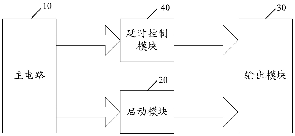
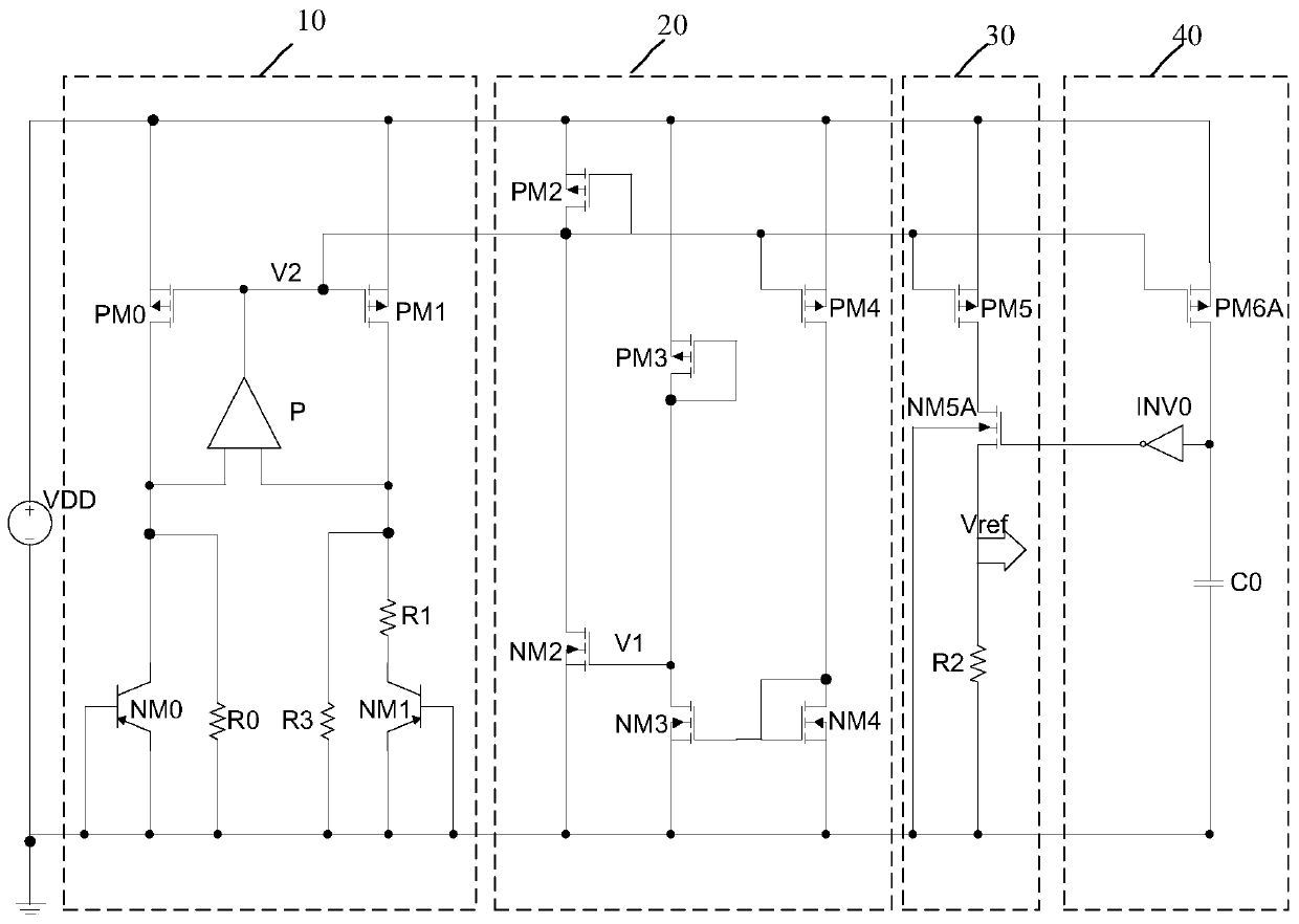
[0029] An embodiment of the present invention provides a bandgap reference circuit, which is suitable for outputting a reference current without overshoot, see figure 1 , the bandgap reference circuit can include:

[0030] The main circuit 10 is connected to the power supply VDD for outputting a reference current.

[0031] The starting module 20 is connected to the main circuit 10 and the power supply VDD respectively, and is used to start the main circuit 10 .

[0032] The output module 30 is connected with the main circuit 10 and is used for outputting a bandgap reference voltage of a required specification according to the reference current provided by the main circuit 10 .

[0033] The delay control module 40 is connected with the main circuit 10 and the output module 30 respectively, and is used to collect the overshoot signal generated by the main circuit 10 in the start-up phase, and delay the output module 30 to the main circuit according to the overshoot signal colle...


PUM


Abstract

The invention discloses a band-gap reference circuit which comprises a main circuit used for outputting reference current, a starting module used for starting the main circuit, an output module used for outputting band-gap reference voltage of a required specification according to the reference current provided by the main circuit, and a delay control module used for collecting an overshoot signalgenerated by the main circuit in a starting stage and controlling the output module to perform stable output according to the acquired overshoot signal. According to the invention, when the overshootsignal generated by the main circuit in the starting stage is sampled by the delay control module and when the time delay output module is controlled to perform time delay on the sampling of the maincircuit, the time delay time is controllable, then the output module can be controlled to perform sampling after the overshoot signal passes, so the overshoot of output voltage can be weakened or eliminated, and the voltage output of the output module is enabled to be stable.

Description

technical field [0001] The invention relates to the field of circuit technology, in particular to a bandgap reference circuit. Background technique [0002] In a conventional bandgap reference circuit, an overshoot occurs during the establishment of the output voltage Vref. Taking the field of NORFLASH (that is, non-volatile flash memory technology) as an example, the common erasing method of NOR FLASH needs to apply a negative pressure to WL. The negative pressure is generated by the negative charge pump inside the chip, and the size is based on the multiple of Vref. -7 times as an example, that is, the WL voltage is -8.4v when erasing, at this time the VDS of the internal levelshift MOS tube is (3.3-(-8.4))=11.7v, in the safe working range (the process determines the drain and source The punch-through voltage is 12.5v); if the overshoot is 0.3v at this time, the VDS of the levelshift MOS is 13.8v, which is greater than the punch-through voltage, which will cause irreversi...

Claims


Application Information

Patent Timeline
Patent Type & Authority Applications(China)
IPC IPC(8): G05F1/56
CPCG05F1/56
Inventor 刘梦
Owner XTX TECH INC
Why Eureka
Try Eureka