Defect detection device and defect detection method

A defect detection and defect technology, applied in measurement devices, optical testing of defects/defects, material analysis by optical means, etc., can solve problems such as easy generation of crosstalk signals, affecting the accuracy of defect detection results, and improve defect detection accuracy. , the effect of suppressing crosstalk

Active Publication Date: 2020-01-07
SHANGHAI MICRO ELECTRONICS EQUIP (GRP) CO LTD
View PDF9 Cites 4 Cited by
  • Summary
  • Abstract
  • Description
  • Claims
  • Application Information

AI Technical Summary

Problems solved by technology

[0004] However, in the process of defect detection of existing defect detection devices, the pattern on the lower surface of the product to be tested is prone to generate crosstalk signals, which affects the accuracy of defect detection results

Method used


Image

  • Defect detection device and defect detection method
  • Defect detection device and defect detection method
  • Defect detection device and defect detection method

Examples


Embodiment Construction

[0047] The present invention will be further described in detail below in conjunction with the accompanying drawings and embodiments. It should be understood that the specific embodiments described here are only used to explain the present invention, but not to limit the present invention. In addition, it should be noted that, for the convenience of description, only some structures related to the present invention are shown in the drawings but not all structures.

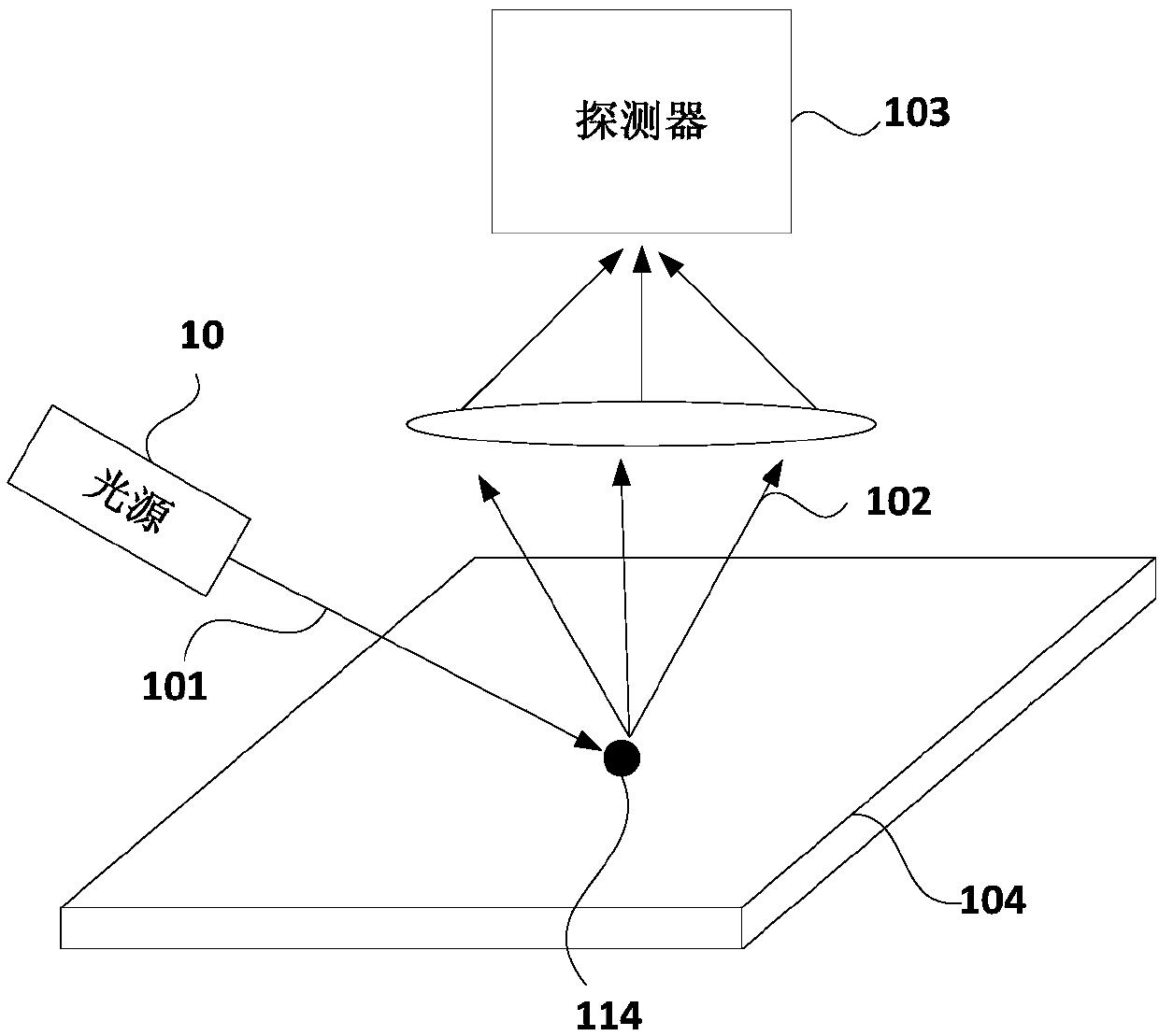
[0048] figure 2 is a schematic structural diagram of the defect detection device provided by the embodiment of the present invention, please refer to figure 2 , the device includes an illumination module 20 and an imaging detection module 30; the illumination module 20 is used to generate a detection beam 201, and makes the detection beam 201 incident on the detection surface of the product 40 to be tested; the imaging detection module 30 is used to detect whether the detection beam 201 Scattered imaging light ...


PUM


Abstract

The invention discloses a defect detection device and a defect detection method. The defect detection device comprises an illumination module and an imaging detection module; the illumination module is used for generating a detection light beam and enabling the detection light beam to be incident on a detection surface of a product to be detected; the imaging detection module is used for detectingwhether the detection light beam is scattered by the detection surface of the product to be detected to generate a scattered imaging light beam or not, and determining defect information of the product to be detected according to the scattered imaging light beam; the illuminance of the detection light beam satisfies that (U1*R) / (U2*L) is greater than or equal to S1; and the half width W of the detection light beam satisfies that d*[tan alpha+ tan beta] is greater than FOV / 2+W. According to the embodiments, the detection light beam generated by the illumination module is determined by determining the relative illuminance between the half-wide edge of the detection light beam and the center of the detection light beam and the half-width of the detection light beam, so that crosstalk generated in the defect detection process is suppressed, and the defect detection precision is improved.

Description

technical field [0001] Embodiments of the present invention relate to the technical field of defect detection, and in particular, to a defect detection device and a defect detection method. Background technique [0002] In the manufacturing process of semiconductor integrated circuits or flat panel displays, in order to maintain a high yield rate of products, defects (including foreign particles, fingerprints, scratches, pinholes, etc.) etc.) to achieve the purpose of pollution control. [0003] figure 1 It is a schematic diagram of the structure of an existing defect detection device. Generally, the particle detection device integrated in the lithography equipment usually adopts the dark field scattering measurement technology, and its detection principle is as follows: figure 1 As shown, the illumination light 101 emitted from the light source 10 is scattered by the defect 114 on the object 104 to be tested, and the scattered light 102 is finally detected by the detector...

Claims


Application Information

Patent Timeline
IPC IPC(8): G01N21/88
CPCG01N21/8806G01N21/88
Inventor 杨晓青申永强韩雪山王帆
Owner SHANGHAI MICRO ELECTRONICS EQUIP (GRP) CO LTD
Why Eureka
Try Eureka