Optical transceiver

a transceiver and optical technology, applied in the field of optical transceivers, can solve the problems of large increase in total cost, large increase in cost, and large increase in cos

Inactive Publication Date: 2005-01-27
SONY CORP
View PDF7 Cites 16 Cited by
  • Summary
  • Abstract
  • Description
  • Claims
  • Application Information

AI Technical Summary

Benefits of technology

[0016] In the optical transceiver according to the present invention, on the end surface of the optical fiber that is inserted into and fixed to the via hole, the light emitting section of the optical integrated chip is opposite through the first waveguide, and the light receiving section is opposite through the second waveguide. Consequently, the transmitting light emitted from the light emitting section is passed through the first waveguide and inputted to the optical fiber, and the receiving light from the optical fiber is passed through the second waveguide and inputted to the light receiving section. Thus, it is possible to attain the single-wire two-way communication of full-duplex, in which the crosstalk is suppressed under the simple structure, since the transmitting light and the receiving light are separated.

Problems solved by technology

Thus, the number of assembling steps was increased to thereby lead to a large increase in cost.
Similarly, a large number of members for adjusting and fixing were required to thereby increase the number of components, which led to the large increase in the cost.
Also, the conventional optical transceiver required a substrate made of silicon that had a V-groove to support the optical fiber, components using expensive materials such as a lens made of glass and the like, and complex processes to make those components.
Hence, the cost of the components and the processing cost were increased to thereby lead to the large increase in the total cost.
This led to increase the number of the components and increase the cost of the components.
Also, the beam splitter that was the optical component for separating the optical path was very expensive, so that this also led to the increase in the total cost of the optical transceiver.
Thus, in order to minimize their errors, the number of the assembling steps, especially, the number of the steps necessary for the adjustment was increased to thereby lead to the large increase in the cost.

Method used


Image

  • Optical transceiver
  • Optical transceiver
  • Optical transceiver

Examples


first embodiment

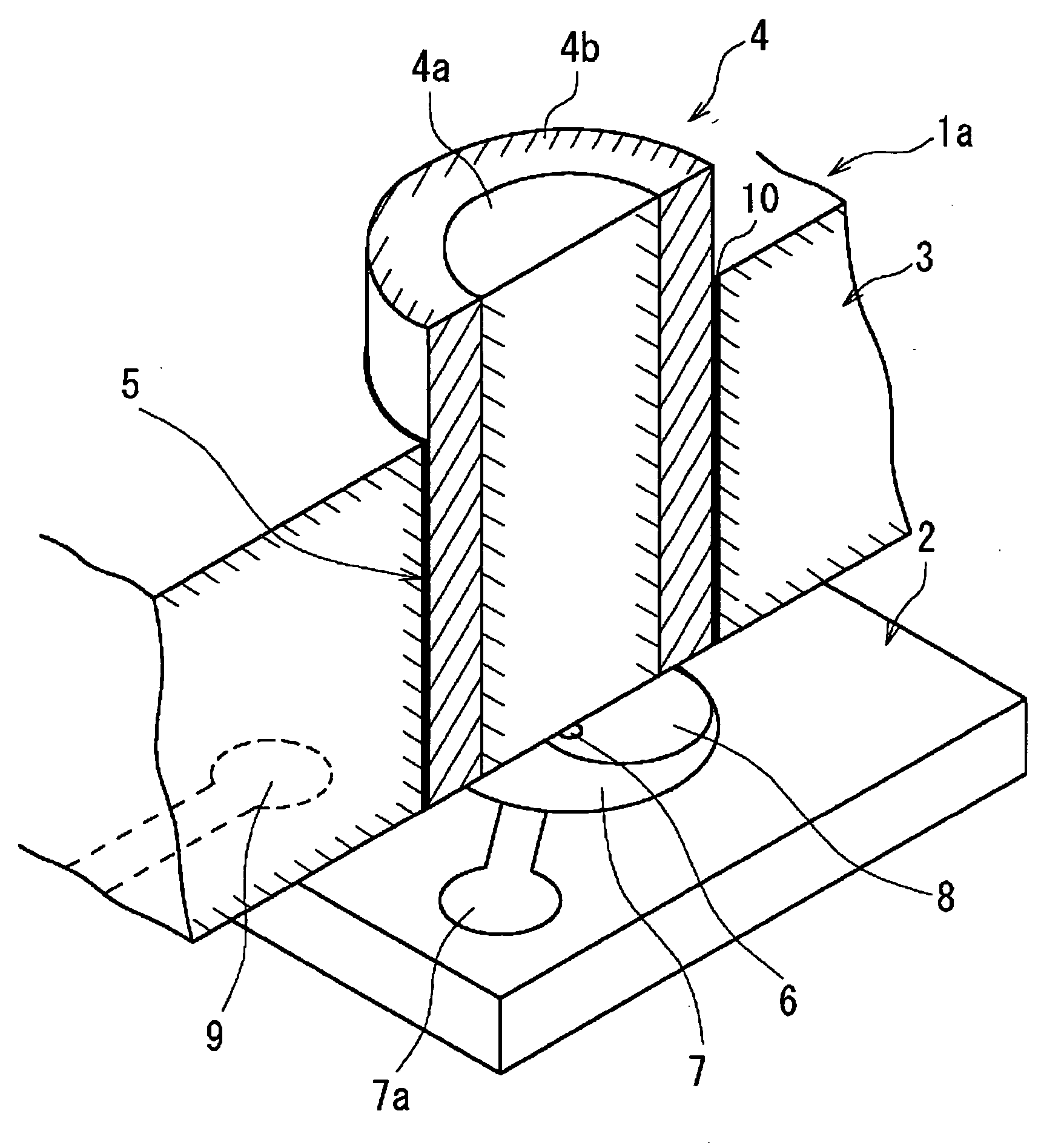
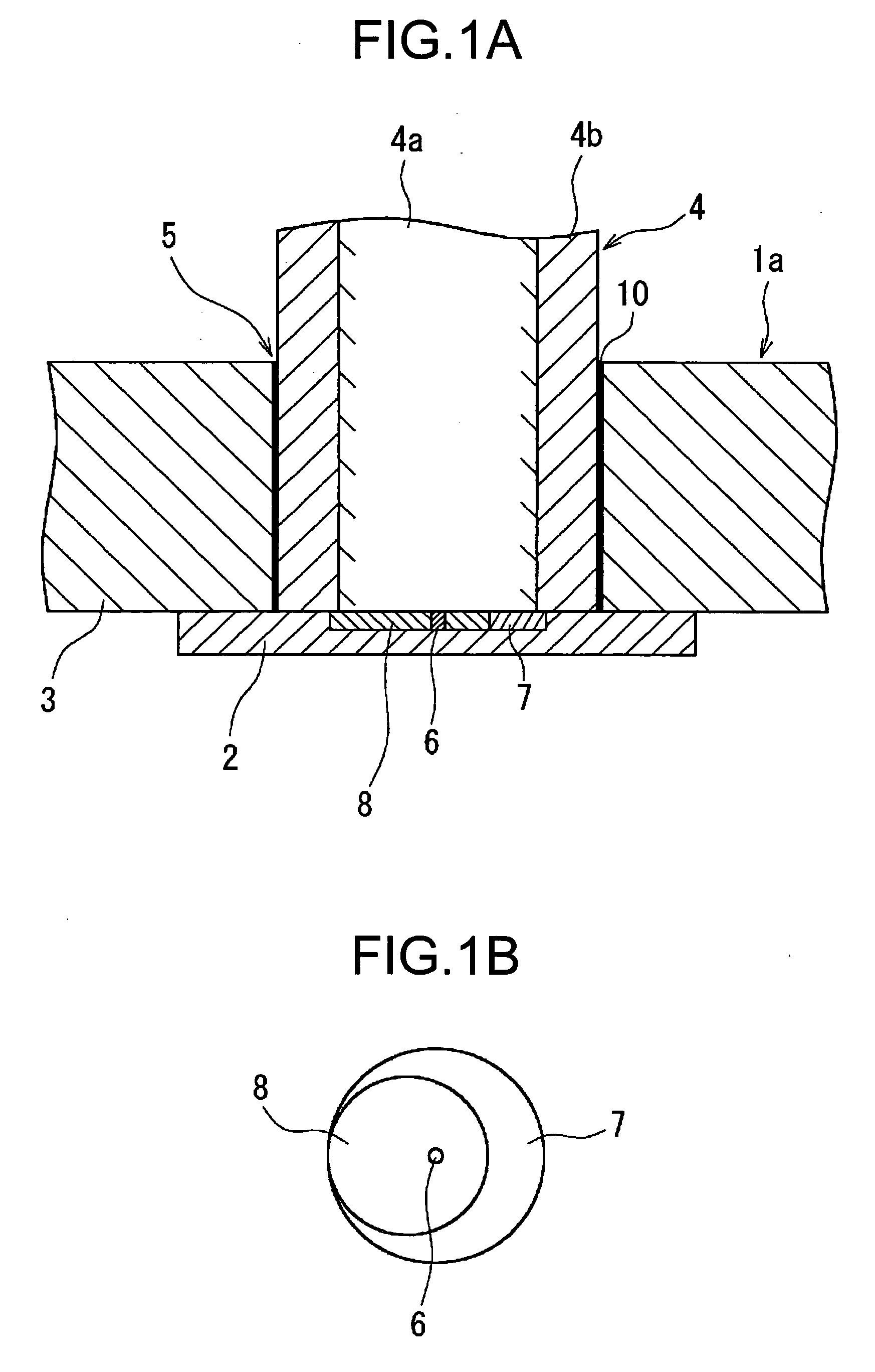
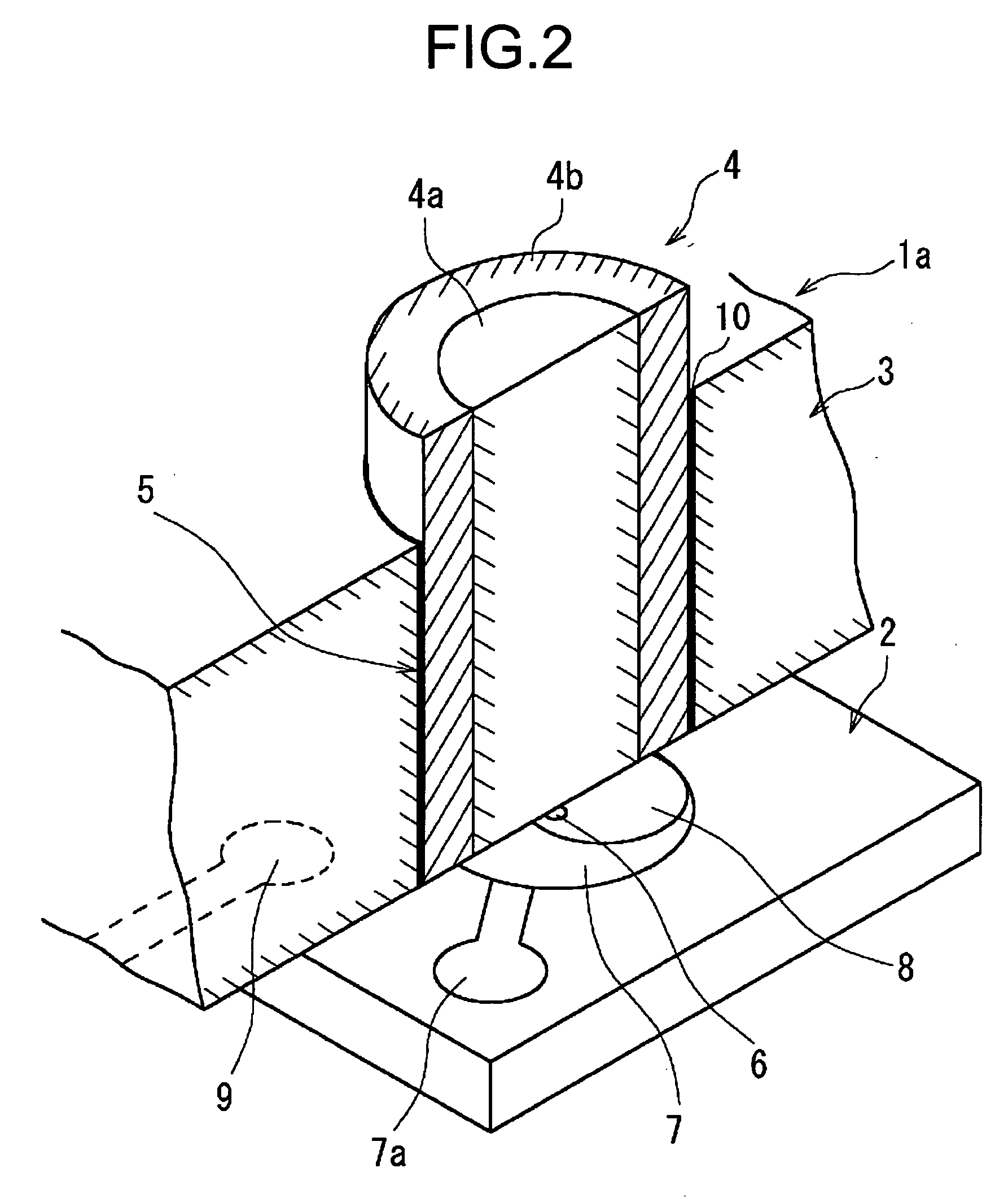
[0039] An optical transceiver 1a in the first embodiment is designed such that an optical integrated chip 2, in which a light emitting element and a light receiving element are formed on the same chip, is mounted as flip-chip mounting on a circuit board 3, and an optical fiber 4 optically coupled with this optical integrated chip 2 is inserted into and fixed to a via hole 5 formed in the circuit board 3.

[0040]FIG. 3 is a perspective view showing the configuration example of the optical integrated chip 2. At first, the configuration of the optical integrated chip 2 is explained. In the optical integrated chip 2, the light emitting element and the light receiving element are formed on the same chip, and a light emitting section 6 and a light receiving section 7 are formed on the surface side of the optical integrated chip 2. The light emitting section 6 is VCSEL (Vertical Cavity Surface Emitting Lasers), namely a flat light emitting element, and the light receiving section 7 is formed...

second embodiment

[0059] An optical transceiver 1b in the second embodiment is designed such that an optical component 11 for separating the paths of the transmitting light and the receiving light is inserted between the optical fiber 4 and the optical integrated chip 2. The optical component 11 is designed such that, for example, metal plating is performed on an outer surface of a glass fiber having a two-layer structure, and a refractive index of an outer layer section is made different from that of an inner layer section. Consequently, the light is confined in the inner layer section, and this inner layer section forms a first waveguide 11a. Also, the outer layer section forms a second waveguide 11b. Thus, a total reflection film 11c is formed on the outer surface of the optical component 11 by the metal plating and the like, and the light is confined. Consequently, the optical component 11 is configured such that the light passed through the first waveguide 11a and the light passed through the se...

third embodiment

[0073] An optical transceiver 1c in the third embodiment is designed such that an optical component 12 for separating the paths of the transmitting light and the receiving light is inserted between the optical fiber 4 and the optical integrated chip 2, and a total reflection film 13 is formed on the inner surface of the via hole 5. In the optical component 12, for example, a total reflection film 12a is formed around a glass tube by metal plating. Then, a first waveguide 12b in which the light is confined is formed on the inner surface of the total reflection film 12a.

[0074] The configuration of the optical integrated chip 2 is as described in FIG. 3. Also, the via hole 5 into which the optical fiber 4 is inserted is penetrated and formed in the circuit board 3. The total reflection film 13 is formed on the inner surface of this via hole 5, for example, by metal plating. A diameter of the optical component 12 is smaller than a diameter of the via hole 5. A gap through which the lig...


PUM


Abstract

This invention provides an optical transceiver that can attain a single-wire two-way communication in a simple structure. In an optical integrated chip, a light emitting element and a light receiving element are formed on the same chip, and a light emitting section and a light receiving section are closely placed. A via hole into which an optical fiber is inserted is penetrated in a circuit board. The optical integrated chip is mounted on a rear of the circuit board, at a position where the light emitting and receiving sections are fitted into the via hole. The optical fiber is inserted into the via hole, from the surface of the circuit board. Thus, light from the light emitting section is inputted to the optical fiber, and light from the optical fiber is inputted to the light receiving section. Hence, the single-wire two-way communication is attained.

Description

CROSS REFERENCE TO RELATED APPLICATION [0001] This application claims priority from Japanese Priority Document No. 2002-355413, filed on Dec. 6, 2002 with the Japanese Patent Office, which document is hereby incorporated by reference. BACKGROUND OF THE INVENTION [0002] 1. Field of the Invention [0003] The present invention relates to an optical transceiver for carrying out a single-wire two-way communication by using an optical fiber. In detail, the present invention particularly relates to an optical transceiver, wherein an optical fiber is fixed by inserting into a via hole formed in a circuit board, and an optical integration chip on which a light emitting element and a light receiving element are formed on the same chip is mounted oppositely to the via hole, and thereby a single-wire two-way communication is carried out in a simple structure. [0004] 2. Description of Related Art [0005] An apparatus for carrying out an optical communication using an optical fiber is provided with...

Claims


Application Information

Patent Timeline
Patent Type & Authority Applications(United States)
IPC IPC(8): G02B6/42
CPCH04B10/40G02B6/4246
Inventor IKEDA, TAKESHI
Owner SONY CORP
Why Eureka
Try Eureka