Preparation method for display substrate, display substrate, display panel and control method
A technology for display substrates and display panels, used in semiconductor/solid-state device manufacturing, electrical components, electro-solid devices, etc., can solve problems such as brightening, and achieve the effects of increasing transmittance, reducing power consumption, and increasing charge migration rate.
- Summary
- Abstract
- Description
- Claims
- Application Information
AI Technical Summary
Problems solved by technology
Method used
Image
Examples
Embodiment 1
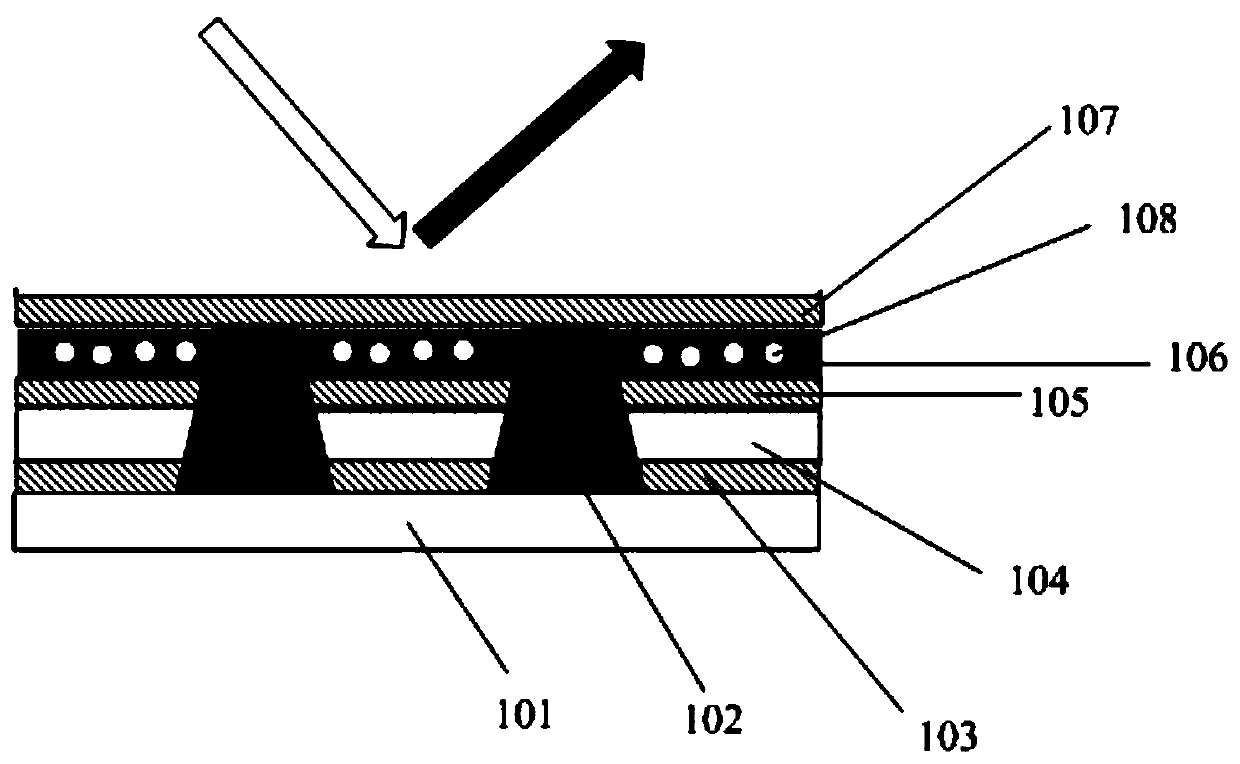
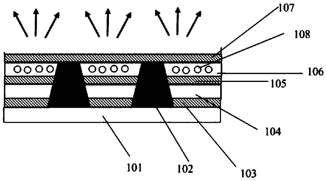
[0036] The display substrate in the present application includes: a substrate, a pixel definition layer located on the substrate, and a first electrode layer, an organic light-emitting layer, a second electrode layer, an electrochromic layer and a first electrode layer stacked on the substrate. three electrode layers.
[0037] Wherein, the first electrode layer is located on the substrate, the electrochromic layer is located between the second electrode layer and the third electrode layer, and between the second electrode layer and the third electrode layer Under the action of the transparent state and the dark state switching.
[0038] In a specific implementation, as an implementation, the first electrode layer, the organic light-emitting layer, the second electrode layer, the electrochromic layer and the third electrode layer can be formed on the entire surface of the pixel definition layer of the substrate, specifically including:
[0039] A substrate is provided.
[004...
Embodiment 2
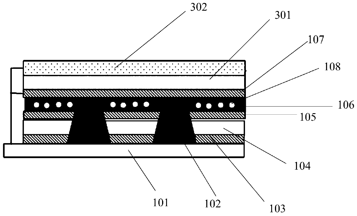
[0074] see image 3 It is a schematic structural diagram of a display panel described in Embodiment 2 of the present application, specifically including: the display substrate described in Embodiment 1 and an encapsulation layer 301 encapsulated on the display substrate.
[0075] The encapsulation layer 301 is covered with a power supply film 302 for supplying power to the third electrode.
[0076] The power supply film is a pressure film or a solar film.
[0077] In practical applications, when the power supply film is a pressure film, the pressure film supplies power to the third electrode layer on the electrochromic layer by converting the external pressure into electrical energy. Since the electrochromic layer belongs to a bistable structure , when the OLED is not displaying, it is necessary to apply a forward voltage to the third electrode layer, so the required power consumption is not large.
[0078] When the power supply film is a solar film, the solar film converts ...
Embodiment 3
[0081] see Figure 4 It is a flowchart of a method for preparing a display substrate described in Embodiment 3 of the present application, including the following steps:
[0082] Step 401: Provide a substrate.
[0083] Step 402 : forming a pixel definition layer, and stacked first electrode layer, organic light emitting layer, second electrode layer, electrochromic layer and third electrode layer on the substrate.
[0084] Wherein, the first electrode layer is located on the substrate, the electrochromic layer is located between the second electrode layer and the third electrode layer, and between the second electrode layer and the third electrode layer Under the action of the transparent state and the dark state switching.
[0085] As one of the implementation manners, step 402 includes the following steps:
[0086] Specifically, a pixel definition layer is formed on the substrate, and a black light-absorbing dye is doped into the pixel definition layer, and the pixel defi...
PUM
 Abstract
Description
Claims
Application Information
 - R&D
- Intellectual Property
- Life Sciences
- Materials
- Tech Scout
- Unparalleled Data Quality
- Higher Quality Content
- 60% Fewer Hallucinations
Browse by: Latest US Patents, China's latest patents, Technical Efficacy Thesaurus, Application Domain, Technology Topic, Popular Technical Reports.
© 2025 PatSnap. All rights reserved.Legal|Privacy policy|Modern Slavery Act Transparency Statement|Sitemap|About US| Contact US: help@patsnap.com


