Optical imaging lens assembly, image capturing unit and electronic device
一种成像光学、镜片组的技术,应用在光学、光学元件、仪器等方向
- Summary
- Abstract
- Description
- Claims
- Application Information
AI Technical Summary
Problems solved by technology
Method used
Image


Examples
no. 1 example
[0129] Please refer to Figure 1 to Figure 2 ,in figure 1 It is a schematic diagram of an imaging device according to the first embodiment of the present invention, figure 2 From left to right are the spherical aberration, astigmatism and distortion curves of the first embodiment. Depend on figure 1 It can be seen that the image capturing device includes an imaging optical lens set (not another number) and an electronic photosensitive element 180 . The imaging optical lens group includes an aperture 100, a first lens 110, a second lens 120, a diaphragm 101, a third lens 130, a fourth lens 140, a fifth lens 150, and an infrared filter from the object side to the image side. Element (IR-cut Filter) 160 and imaging surface 170 . Wherein, the electronic photosensitive element 180 is disposed on the imaging surface 170 . The imaging optical lens set includes five single non-cemented lenses (110, 120, 130, 140, 150), and there is no other interpolated lens between each lens. ...
no. 2 example
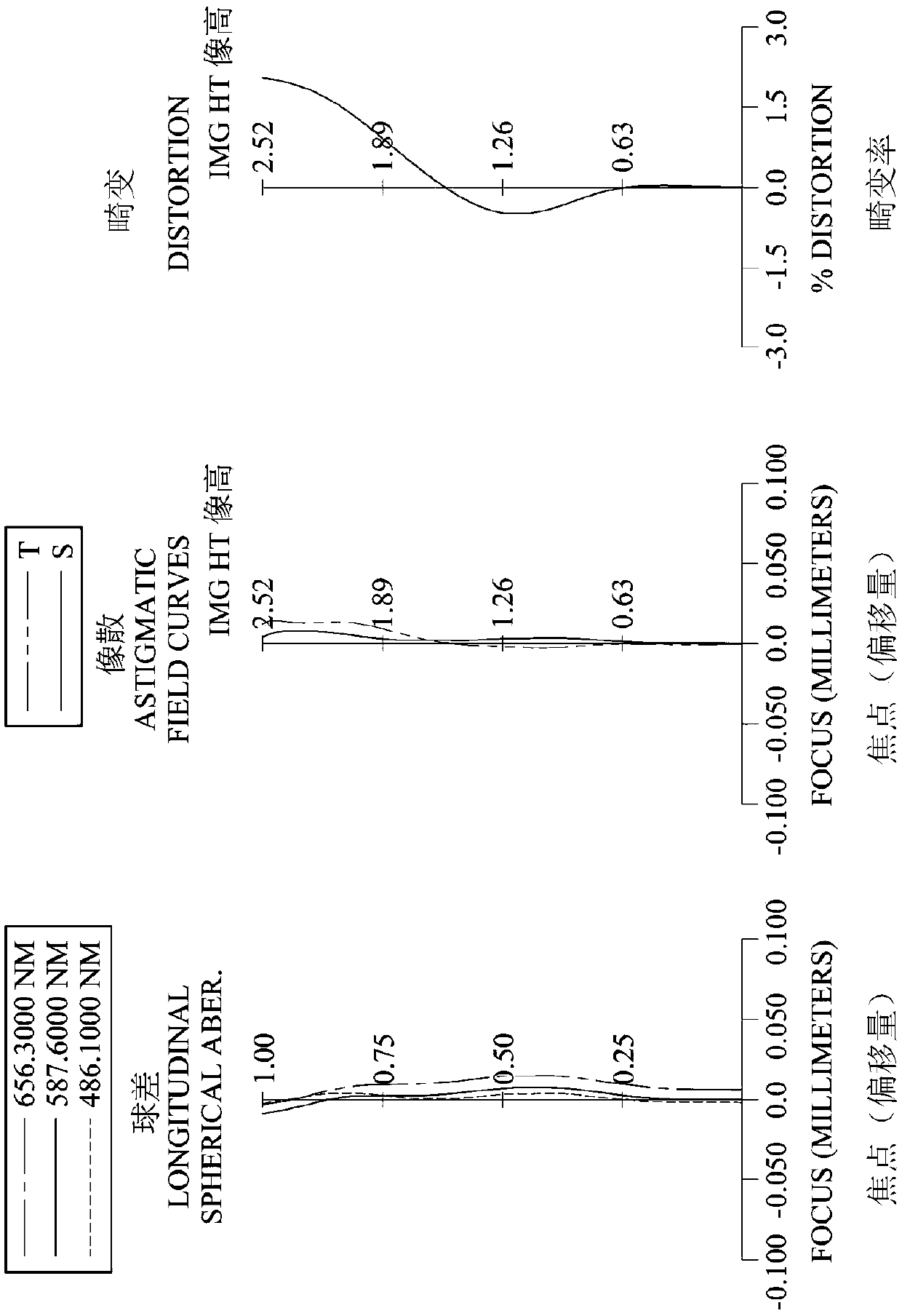
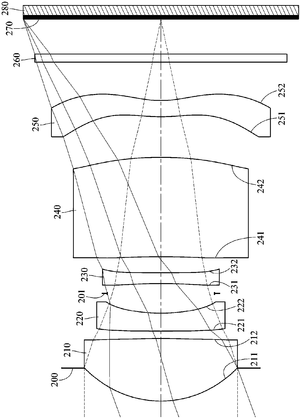
[0165] Please refer to Figure 3 to Figure 4 ,in image 3 It is a schematic diagram of an imaging device according to a second embodiment of the present invention, Figure 4 From left to right are the spherical aberration, astigmatism and distortion curves of the second embodiment. Depend on image 3 It can be seen that the image capturing device includes an imaging optical lens set (not another number) and an electronic photosensitive element 280 . The imaging optical lens group includes aperture 200, first lens 210, second lens 220, diaphragm 201, third lens 230, fourth lens 240, fifth lens 250, infrared filter Element 260 and imaging surface 270 . Wherein, the electronic photosensitive element 280 is disposed on the imaging surface 270 . The imaging optical lens set includes five single non-cemented lenses (210, 220, 230, 240, 250), and there is no other interpolated lens between each lens. Among the five lenses, there is an air space between every two adjacent lenses...
no. 3 example
[0180] Please refer to Figure 5 to Figure 6 ,in Figure 5 It is a schematic diagram of an imaging device according to a third embodiment of the present invention, Figure 6 From left to right are the spherical aberration, astigmatism and distortion curves of the third embodiment. Depend on Figure 5 It can be seen that the image capturing device includes an imaging optical lens set (not another number) and an electronic photosensitive element 380 . The imaging optical lens group includes an aperture 300, a first lens 310, a second lens 320, a diaphragm 301, a third lens 330, a fourth lens 340, a fifth lens 350, and an infrared filter from the object side to the image side. Element 360 and imaging surface 370 . Wherein, the electronic photosensitive element 380 is disposed on the imaging surface 370 . The imaging optical lens set includes five single non-cemented lenses (310, 320, 330, 340, 350) without other intervening lenses between each lens. Among the five lenses, t...
PUM
 Abstract
Description
Claims
Application Information
 - R&D
- Intellectual Property
- Life Sciences
- Materials
- Tech Scout
- Unparalleled Data Quality
- Higher Quality Content
- 60% Fewer Hallucinations
Browse by: Latest US Patents, China's latest patents, Technical Efficacy Thesaurus, Application Domain, Technology Topic, Popular Technical Reports.
© 2025 PatSnap. All rights reserved.Legal|Privacy policy|Modern Slavery Act Transparency Statement|Sitemap|About US| Contact US: help@patsnap.com