A method and structure for injecting spins into a two-dimensional electron gas of Gan-based heterostructures
A two-dimensional electron gas and spin injection technology, which is applied to electrical components, circuits, semiconductor devices, etc., can solve problems such as spin relaxation and lower spin injection efficiency
- Summary
- Abstract
- Description
- Claims
- Application Information
AI Technical Summary
Problems solved by technology
Method used
Image


Examples
Embodiment 1
[0033]The preparation of the spin injection structure and the spin-electric injection are achieved through the following steps:
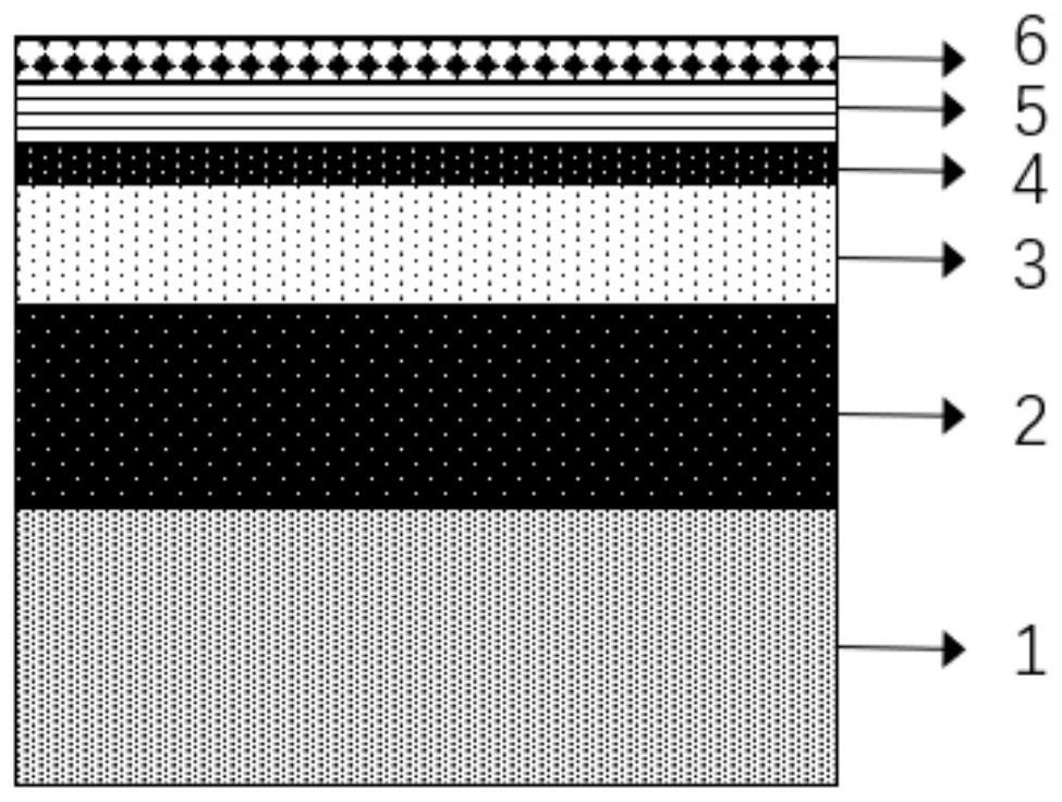
[0034]S1: Use molecular beam epitaxy or metal-organic chemical vapor deposition methods to grow and re-grow GaN layer 2, GaN thin layer 3, and high-quality AlN single crystal layer 4 on substrate 1. In order to prevent AlN oxidation, grow high-quality AlN single crystal After the crystal layer 4, it is necessary to keep the sample in a vacuum environment, and continue to grow the ferromagnetic layer 5 and the protective metal layer 6.
[0035]In the above step S1, the GaN template substrate is grown using MOCVD with a thickness of about 1mm; the high-quality GaN thin layer 3 is grown with MBE with a thickness of about 120nm; the high-quality AlN single crystal layer 4 is grown with MBE with a thickness of about 2nm; the ferromagnetic layer 5 The material of Co is deposited by electron beam with a thickness of 10nm; the material Au of the protective metal layer ...
Embodiment 2
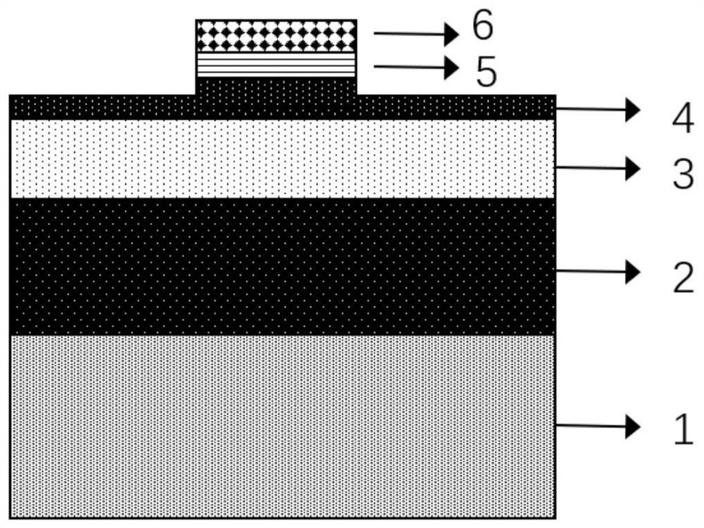
[0038]The steps of this embodiment are basically the same as those of the first embodiment. The difference is that it is difficult to maintain the same vacuum degree for the growth of AlN and the ferromagnetic layer. After the high-quality AlN single crystal layer 4 is grown, hydrogen silsesquioxane (HSQ) is spin-coated in the same vacuum environment, with a thickness of about 200 nm, which is enough to ensure its insulation performance afterwards. Afterwards, the negative electron beam photoresist layer 7 is spin-coated for the stripping of the ferromagnetic metal electrode. Expose the spin injection electrode pattern with an electron beam and develop it so that the AlN under the electrode shape is exposed, and the rest of the HSQ becomes SiO-like2Nature of the protective layer 8, such asimage 3 Shown. In this embodiment, the protective layer 8 is mainly used to prevent oxidation of AlN, and as an insulating layer to isolate the source and drain electrodes and the sample to prevent...
Embodiment 3
[0041]The spin injection junction obtained by the method described in Example 3 can realize the electric spin injection.
[0042]During the experiment of spin-electric injection, it is impossible to guarantee the simultaneous growth of AlN and Co without damaging the vacuum, or the spin-coating of HSQ. In order to minimize the exposure time of AlN in the air, plasma-enhanced chemical vapor deposition (PECVD) was used to grow SiO in the experiment.2Instead of HSQ to protect AlN, there will be several atomic layers of Al on the surface of AlN2O3, But does not affect the effect of the tunneling junction, and spin injection can also be achieved. CorrectFigure 5 The three-terminal spin injection device shown performs low-temperature magnetic transport to measure the effect of spin injection.Figure 5 The IV characteristic characteristic curve of the Au / Co / AlN 2.5nm / GaN tunnel junction shown is as followsFigure 6 As shown, it shows that 2.5nm AlN exhibits one-time tunneling characteristics an...
PUM
| Property | Measurement | Unit |
|---|---|---|
| thickness | aaaaa | aaaaa |
| electrical resistance | aaaaa | aaaaa |
| thickness | aaaaa | aaaaa |
Abstract
Description
Claims
Application Information
 - R&D
- Intellectual Property
- Life Sciences
- Materials
- Tech Scout
- Unparalleled Data Quality
- Higher Quality Content
- 60% Fewer Hallucinations
Browse by: Latest US Patents, China's latest patents, Technical Efficacy Thesaurus, Application Domain, Technology Topic, Popular Technical Reports.
© 2025 PatSnap. All rights reserved.Legal|Privacy policy|Modern Slavery Act Transparency Statement|Sitemap|About US| Contact US: help@patsnap.com