Display device, display substrate thereof, and manufacturing method of display substrate

A technology for display substrates and display areas, which is used in semiconductor/solid-state device manufacturing, semiconductor devices, electrical components, etc., can solve problems such as affecting the overall consistency of the screen, reduce diffraction problems, simplify film structure, and achieve good partition effect. Effect

Active Publication Date: 2021-08-31
KUNSHAN GO VISIONOX OPTO ELECTRONICS CO LTD
View PDF4 Cites 0 Cited by
  • Summary
  • Abstract
  • Description
  • Claims
  • Application Information

AI Technical Summary

Problems solved by technology

[0002] With the rapid development of display devices, users have higher and higher requirements for screen-to-body ratio. Since cameras, sensors, earpieces and other components need to be installed above the screen, a part of the area above the screen is usually reserved in the prior art for the installation of the above-mentioned Components, such as the front notch area of ​​the iPhone X, affect the overall consistency of the screen, and the full-screen display has attracted more and more attention from the industry

Method used


Image

  • Display device, display substrate thereof, and manufacturing method of display substrate
  • Display device, display substrate thereof, and manufacturing method of display substrate
  • Display device, display substrate thereof, and manufacturing method of display substrate

Examples


Embodiment Construction

[0084] In order to make the above objects, features and advantages of the present invention more comprehensible, specific embodiments of the present invention will be described in detail below in conjunction with the accompanying drawings.

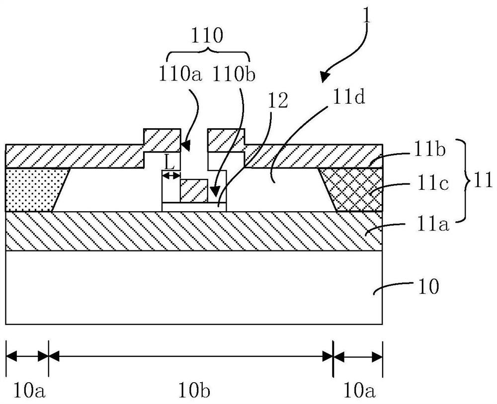
[0085] figure 1 It is a top view of a display substrate in an embodiment of the present invention, wherein the conductive material layer falling on the light-transmitting substrate is removed, and the first pixel definition layer shows a see-through effect; figure 2 is along figure 1 Sectional view of line AA in . image 3 yes figure 1 The schematic diagram of the structure of the display substrate after removing the second electrode in . Figure 4 yes figure 1 The first electrode distribution diagram of the display substrate in .

[0086] refer to Figure 1 to Figure 4 As shown, the display substrate 1 includes a transparent display area 1a, and the transparent display area 1a includes:

[0087] A light-transmitting substrate 10, ...


PUM


Abstract

The present invention provides a display device and its display substrate, and a manufacturing method of the display substrate. In the transparent display area, an opening is made by using a first pixel definition layer between adjacent first sub-pixels, and the opening includes a first sub-pixel from top to bottom. An opening and a second opening, the lateral dimension of the first opening is set to be smaller than the lateral dimension of the second opening, thereby isolating the second electrodes of adjacent first sub-pixels. The opening with a narrow top and a wide bottom has a good isolation effect on conductive materials, and the second electrode adjacent to the first sub-pixel will not be electrically connected; in addition, the isolation column used to isolate the second electrode in the prior art is omitted, which simplifies the transparency. The film layer structure of the display area can reduce the diffraction problem when imaging through the transparent display area.

Description

technical field [0001] The present invention relates to the technical field of display devices, in particular to a display device, a display substrate, and a method for manufacturing the display substrate. Background technique [0002] With the rapid development of display devices, users have higher and higher requirements for screen-to-body ratio. Since cameras, sensors, earpieces and other components need to be installed above the screen, a part of the area above the screen is usually reserved in the prior art for the installation of the above-mentioned Components, such as the front notch area of ​​the iPhone X, affect the overall consistency of the screen, and the full-screen display has attracted more and more attention from the industry. Contents of the invention [0003] The object of the present invention is to provide a display device for a full screen, a display substrate, and a manufacturing method of the display substrate. [0004] In order to achieve the above...

Claims


Application Information

Patent Timeline
Patent Type & Authority Patents(China)
IPC IPC(8): H01L27/32H01L51/52H01L51/56
CPCH10K59/10H10K59/17H10K59/122H10K50/805H10K71/00
Inventor 梁超陶国胜刘如胜
Owner KUNSHAN GO VISIONOX OPTO ELECTRONICS CO LTD
Why Eureka
Try Eureka