Phase focusing image sensor and forming method thereof

An image sensor and phase focusing technology, which is applied in the direction of electric solid-state devices, semiconductor devices, electrical components, etc., can solve the problems of poor performance of phase focusing image sensors, low focusing speed and precision, etc., so as to reduce the photoelectric conversion efficiency and reduce the impact , the effect of performance improvement

Active Publication Date: 2019-08-23
淮安西德工业设计有限公司
View PDF3 Cites 2 Cited by
  • Summary
  • Abstract
  • Description
  • Claims
  • Application Information

AI Technical Summary

Problems solved by technology

[0004] However, since phase focusing needs to use pixels for phase detection, phase focusing has relatively high requirements on light intensity, and the focusing speed and accuracy are not high in dark and weak light environments, resulting in poor performance of phase focusing image sensors.

Method used


Image

  • Phase focusing image sensor and forming method thereof
  • Phase focusing image sensor and forming method thereof
  • Phase focusing image sensor and forming method thereof

Examples


Embodiment Construction

[0029] As mentioned in the background, the performance of prior art phase focusing image sensors is poor.

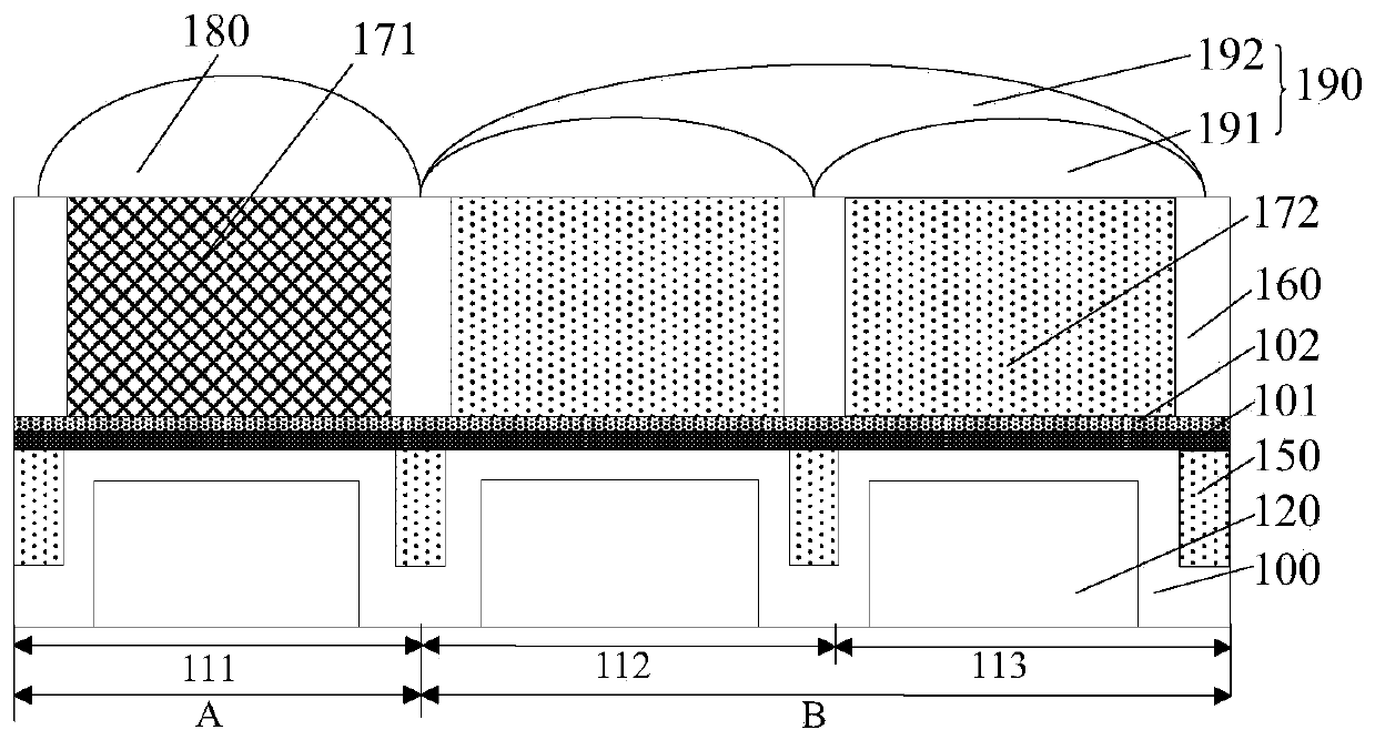
[0030] refer to figure 1 , figure 1 It is a structural schematic diagram of a phase focus image sensor, the phase focus image sensor includes a plurality of image capture units A and a plurality of phase focus units B, and the image capture units A and phase focus units B include: a semiconductor substrate 100, The semiconductor substrate 100 has opposite first and second surfaces; a photosensitive structure 120 located in the semiconductor substrate 100; a photosensitive structure located on the second surface of the semiconductor substrate 100, and the photosensitive structure includes a grid layer 160 , a filter layer and a lens layer; the phase focus image sensor also includes a deep trench isolation layer 150, the second surface of the semiconductor substrate 100 exposes the deep trench isolation layer 150, and the deep trench isolation layer 150 is located In the...


PUM


Abstract

The invention relates to a phase focusing image sensor and a forming method thereof, and the image sensor comprises a semiconductor substrate, wherein the semiconductor substrate comprises an image capture region and a phase focusing region. A first photosensitive layer is arranged in the image capture region of the semiconductor substrate, and a second photosensitive layer is arranged in the phase focusing region of the semiconductor substrate. The image sensor also comprises a first anti-reflection structure which is located on the surface of the semiconductor substrate image capture region;a second anti-reflection structure which is located on the surface of the semiconductor substrate phase focusing area, wherein the reflectivity of the second anti-reflection structure is greater thanthat of the first anti-reflection structure; a first light filtering layer which is located on the surface of the first anti-reflection structure, wherein the monochromatic light passes through the first light filtering layer; and a second light filtering layer which is located on the surface of the second anti-reflection structure, wherein the natural light passes through the second light filtering layer. The performance of the phase focusing image sensor is improved.

Description

technical field [0001] The invention relates to the field of semiconductor manufacturing, in particular to a phase focus image sensor and a forming method thereof. Background technique [0002] An image sensor is a semiconductor device that converts light signals into electrical signals. At present, CMOS phase focusing image sensors have been widely used in digital still cameras, digital video cameras, medical imaging devices, and automotive imaging devices. [0003] At present, the focus methods used in mobile phone shooting are mainly contrast detection autofocus (contrast detection autofocus) and phase detect autofocus (PDAF for short). The principle of contrast focusing is to find the position of the lens with the maximum contrast according to the contrast change of the picture at the focal point, that is, the position of accurate focus. The principle of phase focusing is to reserve some pixels on the photosensitive element for phase detection, and determine the focus ...

Claims


Application Information

Patent Timeline
Patent Type & Authority Applications(China)
IPC IPC(8): H01L27/146
CPCH01L27/1462H01L27/14621H01L27/14627H01L27/14685
Inventor 林永璨内藤逹也
Owner 淮安西德工业设计有限公司
Why Eureka
Try Eureka