Eureka AIR delivers breakthrough ideas for toughest innovation challenges, trusted by R&D personnel around the world.

Dividing device

A workpiece and annular frame technology, applied in the field of splitting devices, can solve the problems of incapable chip spacing, uneven heat shrinkage, etc.

Pending Publication Date: 2019-08-20
DISCO CORP
View PDF1 Cites 0 Cited by
  • Summary
  • Abstract
  • Description
  • Claims
  • Application Information

AI Technical Summary

Problems solved by technology

[0007] However, there is a problem that, as described in the above-mentioned Patent Document 1, when thermal shrinkage is performed in a state where the loose portion of the belt is raised by the pin, the area of ​​the belt after thermal shrinkage follows the shape of the tip of the pin. However, if it is formed into a raised shape, since the slack part of the tape is not uniformly heat-shrunk, it is impossible to make the intervals between the chips equal on the heat-shrunk tape.

Method used


Image

  • Dividing device
  • Dividing device
  • Dividing device

Examples


Embodiment Construction

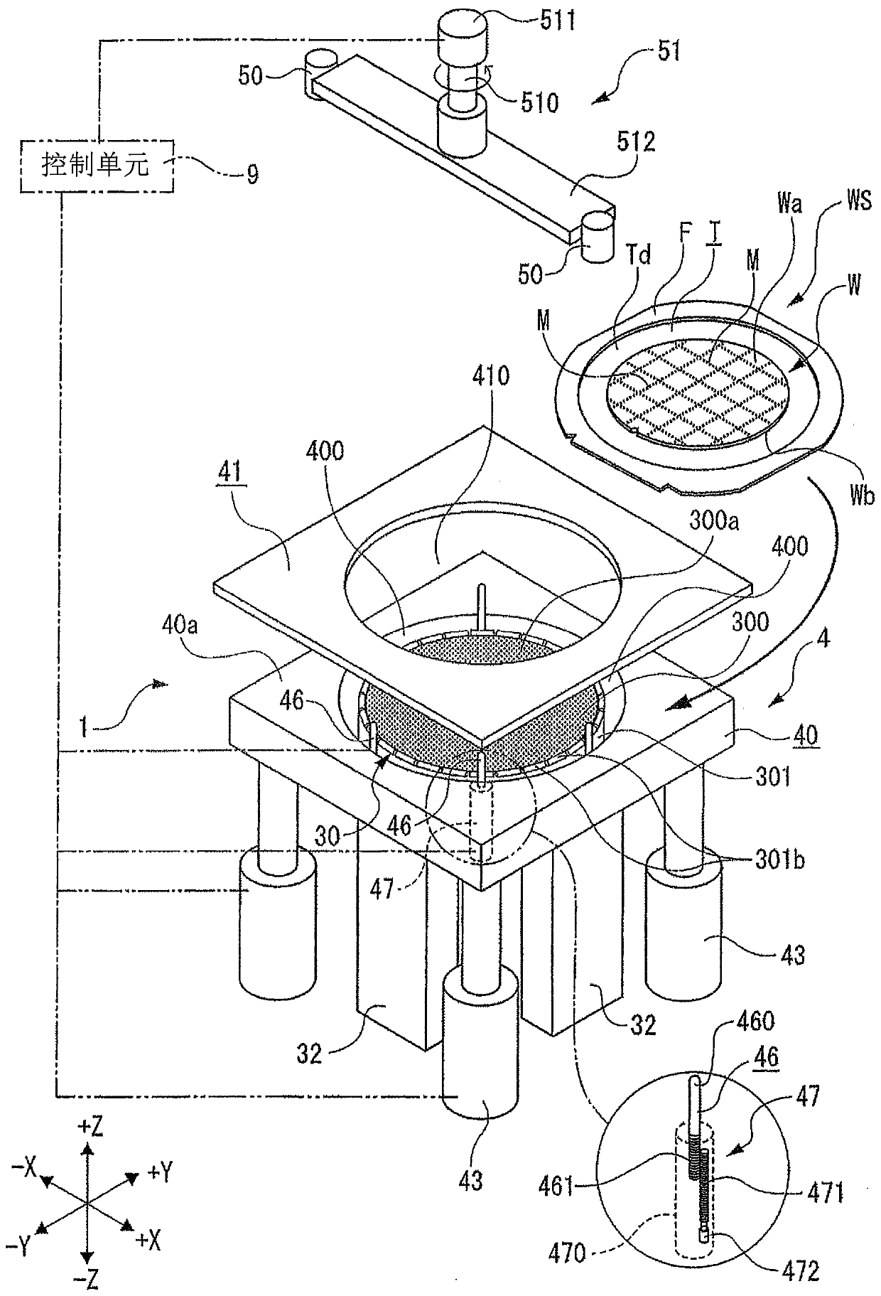
[0032] figure 1 The wafer W shown is, for example, a circular semiconductor wafer made of silicon as a raw material, and a plurality of dividing lines are set vertically on the front surface Wa of the wafer W. Furthermore, devices not shown in the figure are respectively formed in a plurality of grid-like regions partitioned by the planned division lines.

[0033] The wafer W is irradiated with a laser beam of a wavelength transparent to the wafer W along the planned dividing line, and the dividing starting point M (reformed layer M) is continuously formed at a predetermined depth inside the wafer W along the planned dividing line.

[0034] In addition, the division starting point M (modified layer M) is a region where the inside of the wafer W is modified by irradiation of the laser beam so that the intensity is lower than that of the surrounding area. Cracks may extend from the splitting starting point M toward the front Wa or back Wb of the wafer W, respectively. In addit...


PUM


Abstract

The present invention provides a dividing device for dividing a wafer by tape expansion, wherein the chip spacing is kept uniform when the tape is thermally shrunk. The dividing device (1) divides a wafer (W) by expanding a tape (T) of a workpiece group (WS), and comprises: a table (30) for holding a tape (T) of the workpiece group; a frame holding unit (4) that holds the ring frame (F) of the workpiece group on the outside of the table; a lifting unit (43) which makes the worktable and the frame holding part close to or far from each other in the Z-axis direction; a heater (50) which thermally contracts the belt (T) in an annular region (Td) between the outer periphery of the wafer and the inner periphery of the frame; a heater surrounding unit (51); a pin (46) that makes the annular region (Td) of the belt (T) rise and approach the heater (50); and a pin lifting unit (47), wherein the pin (46) is arranged at a preset angle in the circumferential direction by taking the center of thesuction surface of the workbench as the center, and the pin lifting unit (47) is controlled to enable the pin (46) to be slightly far away from the belt (T) when the surrounding heater (50) is positioned right above the pin (46) to enable the belt (T) to be thermally contracted.

Description

technical field [0001] The present invention relates to a dividing device for dividing a wafer into individual chips. Background technique [0002] In the case of dividing a workpiece such as a semiconductor wafer into individual chips along planned dividing lines, for example, a modified layer is formed by irradiating the inside of the wafer with a laser beam transparent to the wafer, and then by applying an external force to the modified layer Instead, the wafer is divided into chips. [0003] For example, the wafer on which the modified layer is formed is attached to a tape having a larger diameter than the wafer, and then the outer peripheral portion of the adhesive surface of the tape is attached to a ring-shaped frame with a circular opening, so that the wafer is held by the tape. The state of the ring frame support. Then, by expanding the tape, an external force (stretching force of the tape) is applied to the modified layer of the wafer attached to the tape, thereb...

Claims


Application Information

Patent Timeline
IPC IPC(8): H01L21/67H01L21/78
CPCH01L21/67092H01L21/78H01L21/67132H01L21/6836H01L21/67103H01L21/6838
Inventor 植木笃政田孝行
Owner DISCO CORP
Why Eureka
Eureka Blog
Learn More