
Microparticle manufacturing device and microparticle manufacturing method

A technology for manufacturing devices and particles, applied in chemical instruments and methods, transportation and packaging, and control/regulating processes, etc., can solve problems such as low processing efficiency, and achieve higher evaporation efficiency, reduction of untreated materials, and increased production. Effect

Active Publication Date: 2019-08-16
PANASONIC INTELLECTUAL PROPERTY MANAGEMENT CO LTD
View PDF8 Cites 2 Cited by
  • Summary
  • Abstract
  • Description
  • Claims
  • Application Information

AI Technical Summary

Problems solved by technology

[0011] However, if the discharge is only from the electrode E1 to the electrode E6, completely unprocessed (unprocessed) material will be generated or the temperature will not be enough to evaporate and the material will be melted, and there will be a problem of low processing efficiency.

Method used


Image

  • Microparticle manufacturing device and microparticle manufacturing method
  • Microparticle manufacturing device and microparticle manufacturing method
  • Microparticle manufacturing device and microparticle manufacturing method

Examples


no. 1 Embodiment approach

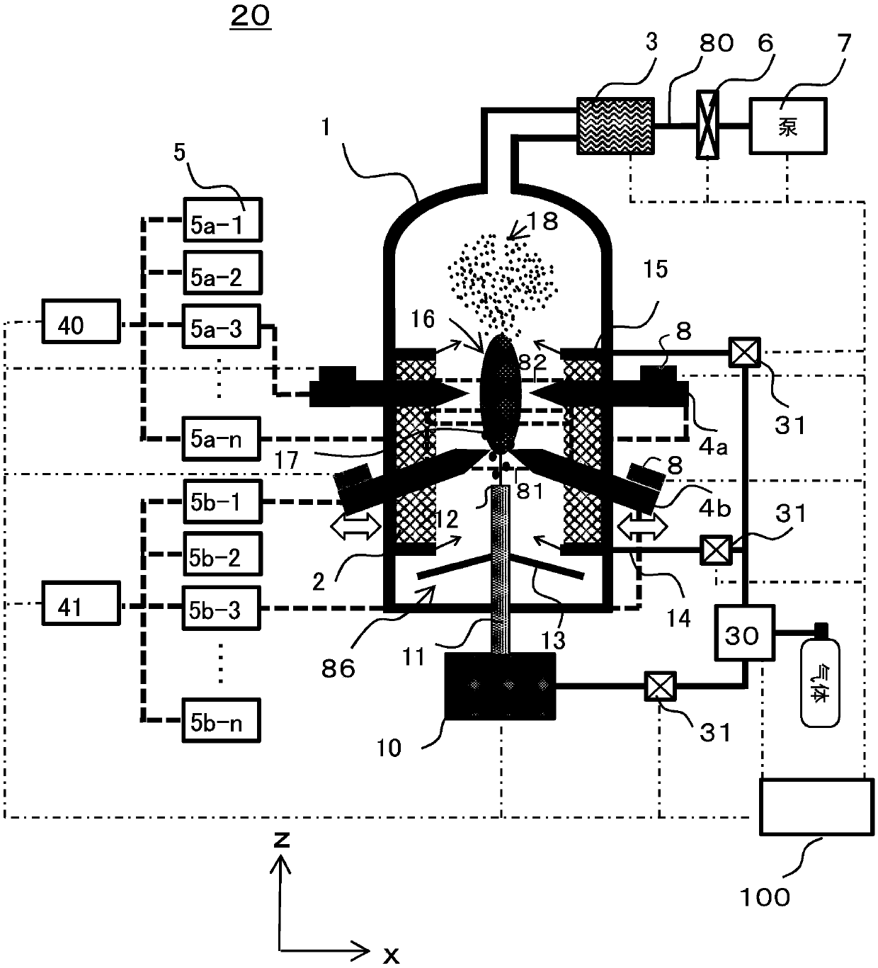
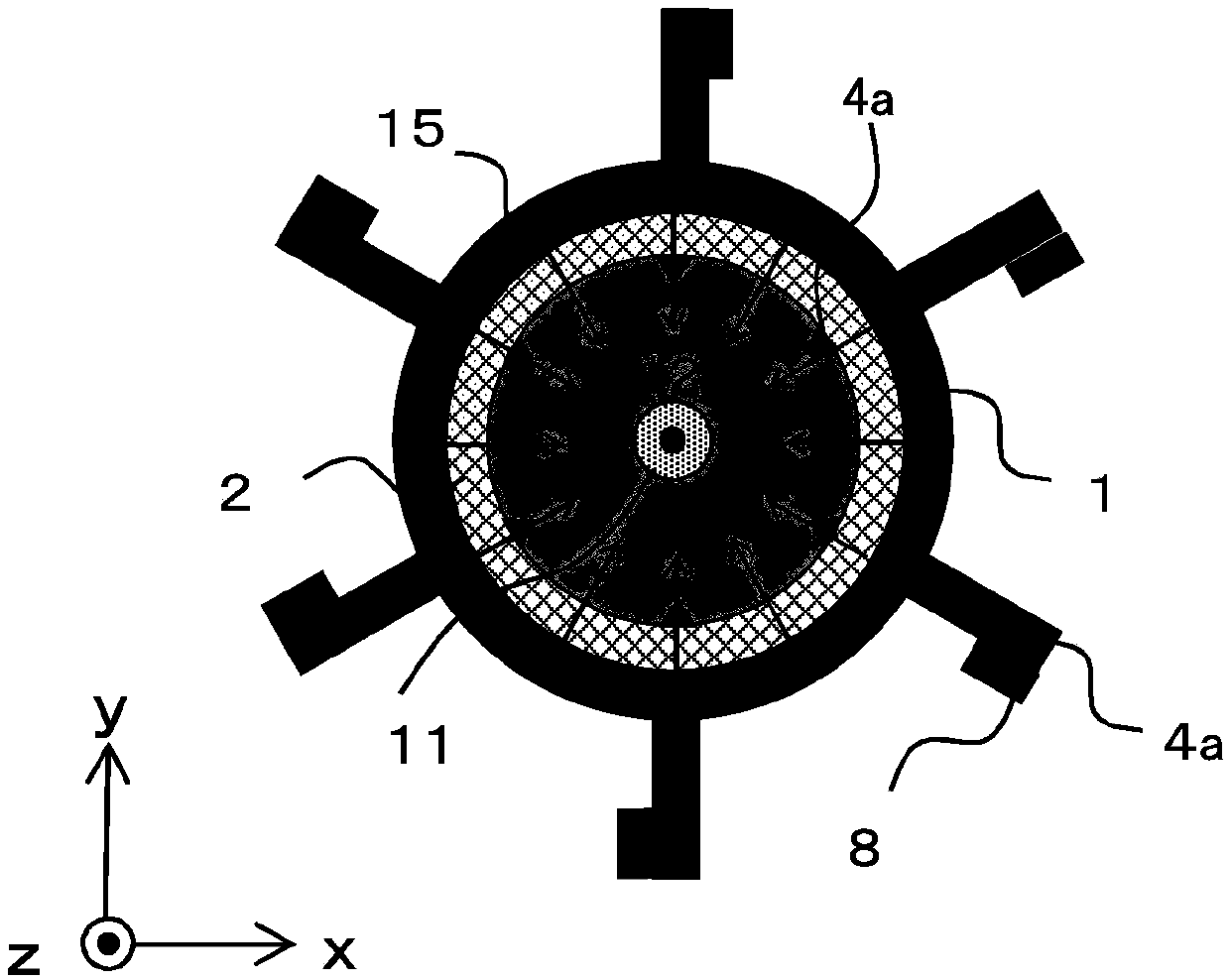
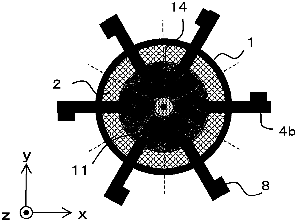
[0064] figure 1 A schematic cross-sectional view of the microparticle manufacturing apparatus 20 according to the first embodiment viewed from a direction perpendicular to the vertical direction is shown. Figure 2A It is a schematic partial cross-sectional view (x-y plan view) seen from the +z direction in the second electrode arrangement region in the vicinity of the upper electrode in the microparticle manufacturing apparatus according to the first embodiment. Figure 2B It is a schematic partial cross-sectional view (x-y plan view) seen from the +z direction in the first electrode arrangement region in the vicinity of the lower electrode. In addition, for the sake of convenience, let one direction in the horizontal plane be the x direction, and let the vertical upper direction be the z direction. use figure 1 , Figure 2A as well as Figure 2B , as an example, an example of producing nanoscale particles of silicon will be described.

[0065] The microparticle produc...


PUM


Abstract

The present invention provides a microparticle production device and a microparticle manufacturing method. The device includes a reaction chamber that extends from the lower side to the upper side inthe vertical direction; a material supply device that supplies material particles to the reaction chamber from a material supply port to the vertical direction; a first electrode arrangement region having a plurality of lower electrodes on an inner peripheral wall of the reaction chamber; a second electrode arrangement region having a plurality of upper electrodes on the part closer to the vertical direction on the inner peripheral wall of the reaction chamber than the first electrode arrangement region; a recycling part connected to the other end side of the vertical upper side in the reaction chamber to collect microparticles; a power source which is capable of changing the frequency of the alternating current power applied to at least one of the lower electrode and the upper electrode;and a control unit which set the frequency of the alternating current power applied to the lower electrode to be the frequency higher than the frequency of the alternating current power applied to theupper electrode. Arc discharge is generated through the lower electrode and the upper electrode, so plasma is generated in the reaction chamber, and microparticles are generated from the material particles.

Description

technical field [0001] The present invention relates to a microparticle production apparatus and a microparticle production method used, for example, as electrode materials of lithium ion batteries, catalyst materials, coating materials such as film materials for food packaging, ink raw materials used in electronic device wiring, and the like. Background technique [0002] In recent years, nanoscale particles have been studied for use in various devices. For example, metal fine particles of nickel are currently used in ceramic capacitors, and the use of fine particles having a particle diameter of 200 nm or less and good dispersibility has been studied for next-generation ceramic capacitors. [0003] Furthermore, fine particles of silicon monoxide (SiOx: x=1 to 1.6) having a lower oxygen content than silicon dioxide are widely used as vapor deposition materials for antireflection films for optical lenses and gas barrier films for food packaging. Recently, applications to ne...

Claims


Application Information

Patent Timeline
Patent Type & Authority Applications(China)
IPC IPC(8): B01J19/08B22F1/054B22F1/065
CPCB01J19/088B01J19/0053B01J19/0006B01J2219/0894B01J2219/0809B01J2219/0815B01J2219/0845B01J2219/0869B01J2219/0879B22F1/054B22F1/065B22F1/056B22F9/14B22F2999/00B01J19/06B01J19/0013B01J2219/0801B01J2219/0841B01J2219/0898B22F3/003B22F2202/13B22F2304/05
Inventor 永井久雄小岩崎刚大熊崇文
Owner PANASONIC INTELLECTUAL PROPERTY MANAGEMENT CO LTD
Learn More