
Graph optimization method and mask preparation method

An optimization method and mask technology, applied in the semiconductor field, can solve problems such as affecting device performance and small adjustability

Active Publication Date: 2019-08-13
SEMICON MFG INT (SHANGHAI) CORP +1
View PDF5 Cites 1 Cited by
  • Summary
  • Abstract
  • Description
  • Claims
  • Application Information

AI Technical Summary

Problems solved by technology

[0003]Due to the small size of the graphics involved in the photolithography process, it is more likely to be affected by optical effects, especially the size of some key graphics, which is less adjustable. If there is a large fluctuation, it will seriously affect the performance of the device

Method used


Image

  • Graph optimization method and mask preparation method
  • Graph optimization method and mask preparation method
  • Graph optimization method and mask preparation method

Examples


Embodiment Construction

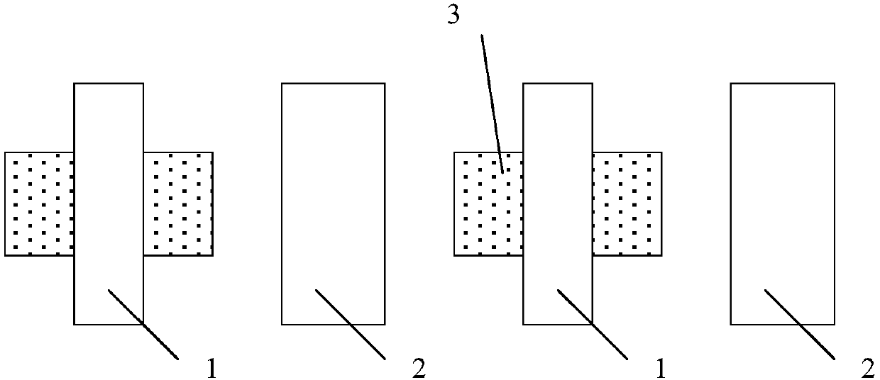
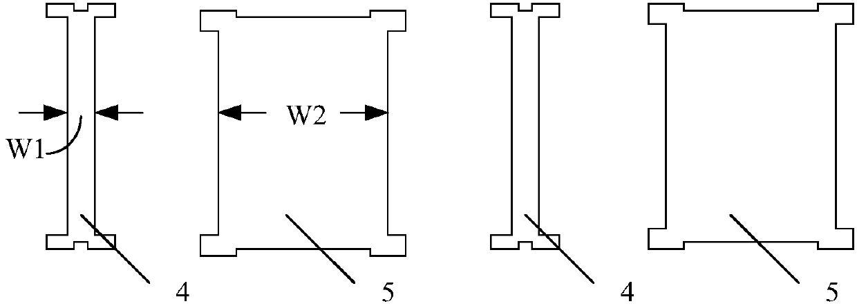
[0029] The graphic optimization method and mask preparation method of the present invention will be described in more detail below in conjunction with schematic diagrams, wherein a preferred embodiment of the present invention is shown, and it should be understood that those skilled in the art can modify the present invention described here and still achieve Advantageous effects of the present invention. Therefore, the following description should be understood as the broad knowledge of those skilled in the art, but not as a limitation of the present invention.

[0030] In the following paragraphs the invention is described more specifically by way of example with reference to the accompanying drawings. Advantages and features of the present invention will be apparent from the following description and claims. It should be noted that all the drawings are in a very simplified form and use imprecise scales, and are only used to facilitate and clearly assist the purpose of illus...


PUM


Abstract

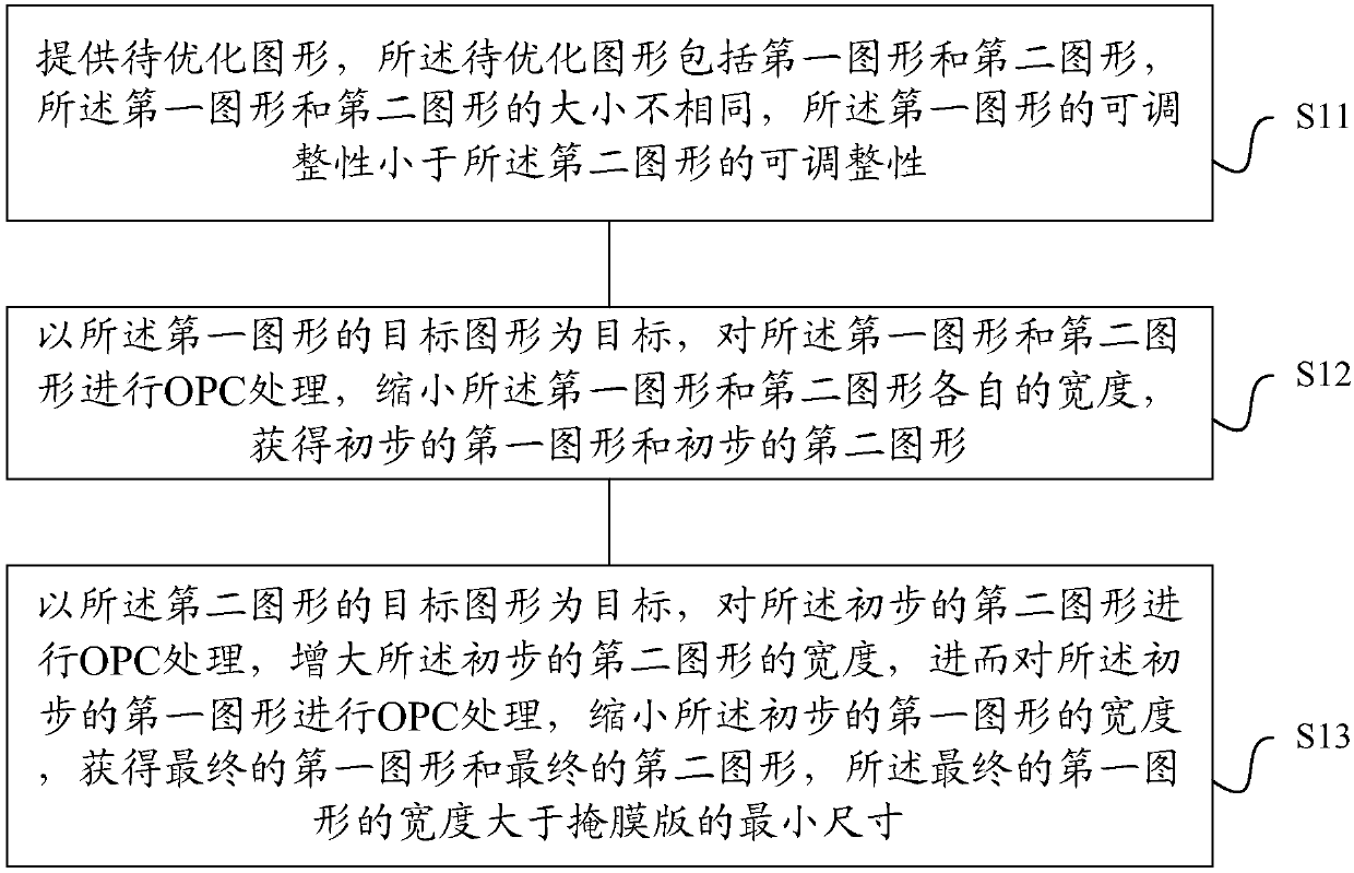
The invention discloses a graph optimization method. The graph optimization method comprises the following steps: providing a to-be-optimized graph, wherein the to-be-optimized graph comprises a firstgraph and a second graph and the first graph and the second graph are different in size; carrying out OPC processing on a first graph with low adjustability; performing OPC processing on the second graph; and meanwhile, adaptively adjusting the first graph. Thus, the width of the final first graph is greater than the minimum size of the mask on the basis of ensuring that the final first graph isrelatively accurate, the condition that the width of the final first graph is close to the minimum size of the mask is avoided, and the graph optimization difficulty is also reduced. Therefore, the quality of the mask plate can be improved through the mask preparation.

Description

technical field [0001] The invention relates to the technical field of semiconductors, in particular to a pattern optimization method and a mask plate preparation method. Background technique [0002] The photolithography process is one of the important links in the semiconductor manufacturing process. Its main process is to enlarge the pattern prepared on the mask plate (also known as the mask) to the substrate after a certain magnification with the help of precision instruments, so as to realize Fabrication of circuit devices. [0003] Due to the small size of the graphics involved in the lithography process, it is more likely to be affected by optical effects, especially the size of some key graphics, which is less adjustable, and if there is a large fluctuation, it will seriously affect the performance of the device. Therefore, how to make the mask pattern, especially the key pattern, more accurate has become a difficult problem that the industry has been paying attenti...

Claims


Application Information

Patent Timeline
IPC IPC(8): G03F1/36
CPCG03F1/36
Inventor 王健杜杳隽温永明
Owner SEMICON MFG INT (SHANGHAI) CORP
Learn More