
Novel back contact heterojunction battery and manufacturing method thereof

A technology of heterojunction cells and manufacturing methods, which is applied in the field of solar cells, can solve the problems of inapplicability to large-scale mass production, complicated and lengthy process flow, and low production capacity per unit time, so as to reduce performance damage and the complexity of alignment, The effect of simple operation steps and shortened production process

Inactive Publication Date: 2019-07-23
GOLD STONE (FUJIAN) ENERGY CO LTD
View PDF9 Cites 5 Cited by
  • Summary
  • Abstract
  • Description
  • Claims
  • Application Information

AI Technical Summary

Problems solved by technology

[0003] However, there are many difficulties in the manufacturing process of back-contact heterojunction solar cells: 1) The process flow is complex and lengthy, requiring multiple wet chemical etching and cleaning, and the amorphous silicon film layer is easily damaged by immersion in acid or alkali solution. and lose the original activity and quality; 2) Form cross-arranged N-type regions and P-type regions on the back, and the two regions need to be completely isolated and insulated to avoid contact short circuits that seriously affect the performance of the battery. Therefore, either in the process of coating Use a mask to prevent the two polarities of the film from overlapping each other, resulting in carrier recombination; mask operation and strict alignment requirements, so the production capacity per unit time is low and the production cost is high, and it is not suitable for large-scale mass production

Method used


Image

  • Novel back contact heterojunction battery and manufacturing method thereof
  • Novel back contact heterojunction battery and manufacturing method thereof
  • Novel back contact heterojunction battery and manufacturing method thereof

Examples


Embodiment

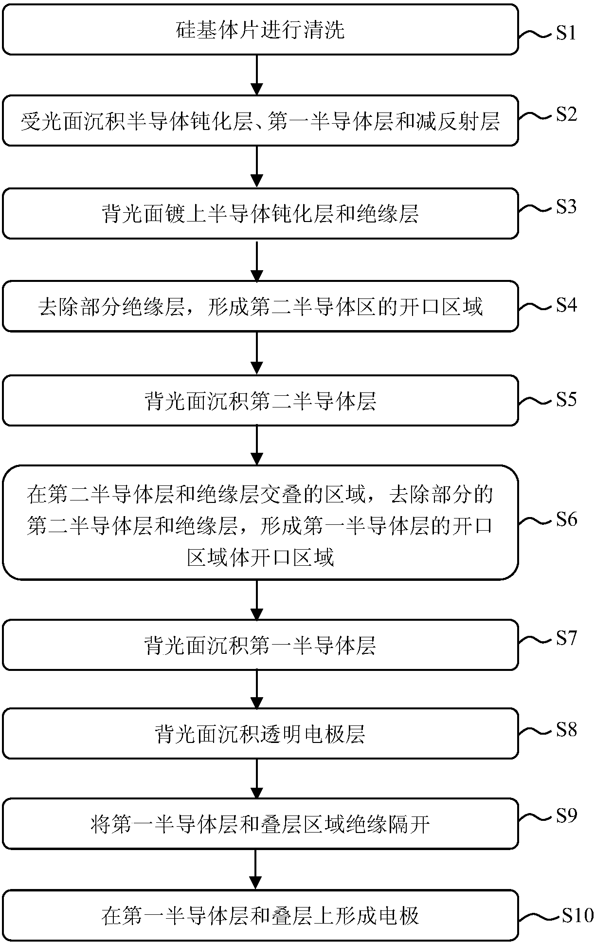
[0034] Such as figure 1 As shown, a new type of back-contact heterojunction cell includes a silicon base sheet 1, the light-receiving surface of the silicon base sheet 1 is sequentially provided with a semiconductor passivation layer 2i, a first semiconductor layer 2n and an anti-reflection layer 3, the The backlight surface of the silicon substrate sheet 1 is provided with a semiconductor passivation layer 4i, and on the semiconductor passivation layer 4i, first semiconductor layers 4n, second semiconductor layers 4p and stacked layers 4np of the first semiconductor layers 4n are alternately arranged. The layer 4n and the laminated layer 4np are respectively provided with a transparent conductive film layer 6, and the transparent conductive film layer 6 is provided with an electrode 7, and an insulating isolation layer is provided between the first semiconductor layer 4n and the laminated layer 4np, and the second An interband tunneling contact is formed between the semicondu...


PUM


Abstract

The invention discloses a novel back contact heterojunction battery and a manufacturing method thereof. The novel back contact heterojunction battery comprises a silicon substrate piece, wherein a semiconductor passivation layer, a first semiconductor layer and an antireflection layer are sequentially arranged on the light receiving surface of the silicon substrate piece, and the semiconductor passivation layer is arranged on the backlight surface; the first semiconductor layer and the laminated layer of a second semiconductor and a first semiconductor are arranged on the semiconductor passivation layer in a staggered mode; a transparent conductive thin film layer is arranged on the first semiconductor layer and the laminated layer separately; an electrode is arranged on the transparent conductive thin film layer; an insulating isolation layer is arranged between the first semiconductor layer and the laminated layer; and inter-band tunneling contact is formed between the second semiconductor layer and the first semiconductor layer. The manufacturing method is simple in operation steps, the first semiconductor layer directly covers the second semiconductor layer, and secondary masketching is not needed, so that the performance damage and complexity of alignment caused by multiple times of masking and etching in the manufacturing process is reduced, and the method is suitable for large-scale production requirements in the future.

Description

technical field [0001] The invention relates to the field of solar cells, in particular to a novel back contact heterojunction cell and a manufacturing method thereof. Background technique [0002] Improving the conversion efficiency of industrial production of solar cells is the future trend of the development of solar energy industry and gradually replacing traditional energy sources. The improvement of cell conversion efficiency mainly improves the electrical parameters such as open circuit voltage, fill factor and short circuit current density; in heterojunction solar cells, by inserting a layer of intrinsic non- The crystalline silicon layer greatly improves the surface passivation effect of the base silicon, and can obtain higher minority carrier lifetime and open circuit voltage, thereby improving the conversion efficiency. In the back contact cell, the electrodes are all distributed on the back, that is, the P pole and the N pole are arranged crosswise on the back o...

Claims


Application Information

Patent Timeline
Patent Type & Authority Applications(China)
IPC IPC(8): H01L31/0747H01L31/20
CPCH01L31/0747H01L31/202Y02E10/50Y02P70/50
Inventor 林锦山谢志刚王树林林朝晖
Owner GOLD STONE (FUJIAN) ENERGY CO LTD
Learn More