Display panel, driving method thereof and display device
A technology of display panel and driving method, applied in static indicators, instruments, etc., can solve problems such as insufficient Pixel charging, increased RCLoading, and shortened MUX turn-on time.
- Summary
- Abstract
- Description
- Claims
- Application Information
AI Technical Summary
Problems solved by technology
Method used
Image
Examples
Embodiment 1
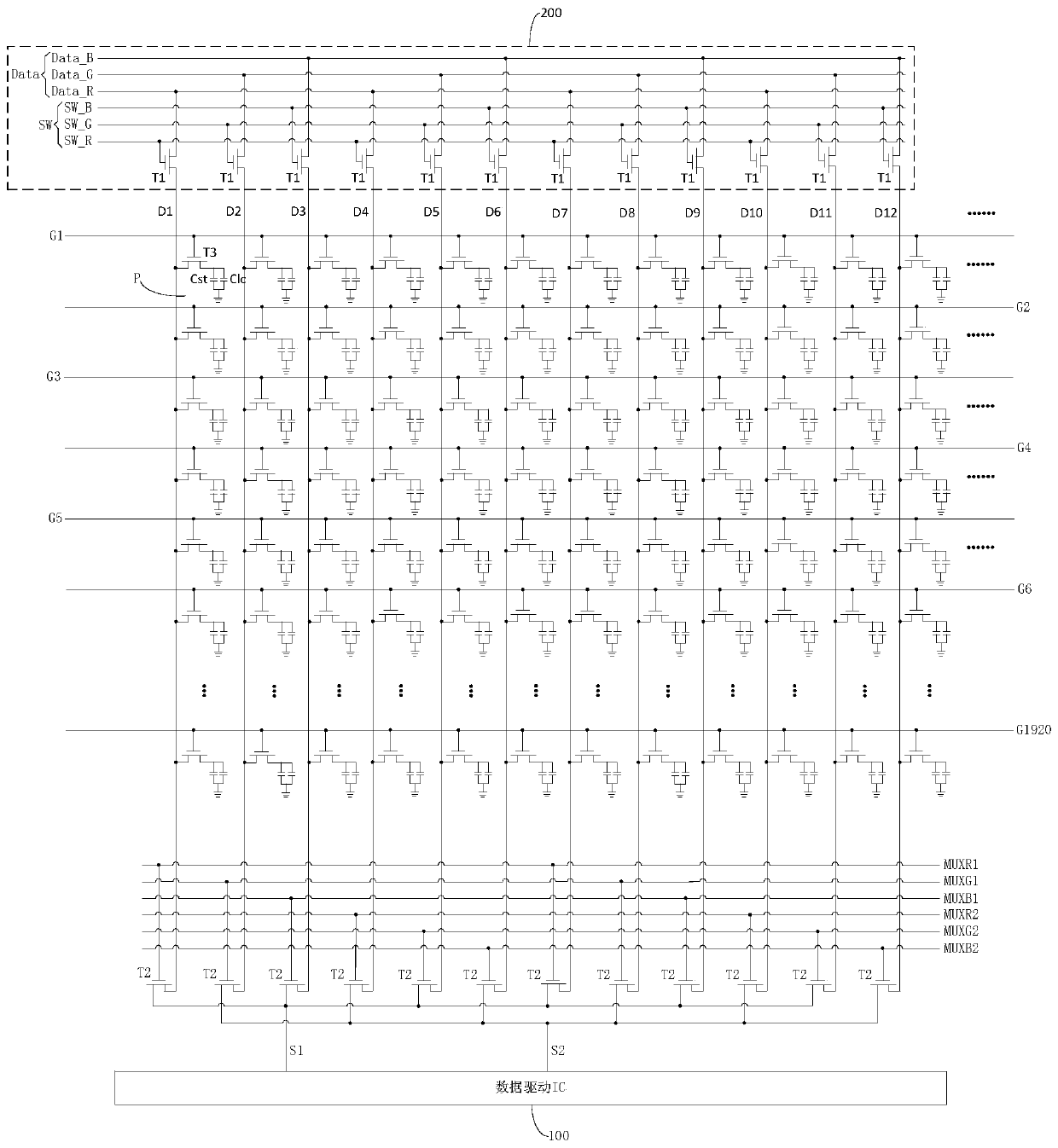
[0047] If it is determined that the frame to be displayed is a solid-color picture, the data driver IC will send an instruction to display a solid-color picture to its internal Flash, and cooperate with each signal (STVL, STVR, CKL, CKR, CKBL, CKBR) in the gate drive circuit to realize The output of the scanning signal, that is, during the scanning period of all the gate lines (from the output of the first row of gate lines to the period of the output of the last row of gate lines), for example, control the sub-control signal line SW_R and the corresponding sub-data compensation line Data_R to input high-level signals , or control the sub-control signal line SW_G and the corresponding sub-data compensation line Data_G to input a high-level signal, or control the sub-control signal line SW_B and the corresponding sub-data compensation line Data_B to input a high-level signal, such as Figure 5 As shown, all switching transistors T1 corresponding to the sub-pixel columns of the s...
Embodiment 2
[0049] If it is judged that the frame picture to be displayed is a heavy-duty picture, the data driver IC will send an instruction to display the heavy-duty picture to its internal Flash. ) To alternately output high and low level signals, taking one line bright and one line dark as an example, the row or column sub-pixels corresponding to the bright screen display a high-level signal to control all switching transistors T1 to conduct, and the sub-pixel columns corresponding to a dark screen input a low voltage The flat signal controls all switching transistors T1 to be cut off, and the high and low level output time of each row control sub-control signal line (SW_R, SW_G, and SW_B) is the same as the output time of the scanning signal, and cooperates with each signal in the gate drive circuit (STV, CK) realizes the output of the scan signal, that is, during the scan period of all gate lines (from the first row of gate line output to the last row of gate line output), control e...
PUM
 Abstract
Description
Claims
Application Information
 - R&D
- Intellectual Property
- Life Sciences
- Materials
- Tech Scout
- Unparalleled Data Quality
- Higher Quality Content
- 60% Fewer Hallucinations
Browse by: Latest US Patents, China's latest patents, Technical Efficacy Thesaurus, Application Domain, Technology Topic, Popular Technical Reports.
© 2025 PatSnap. All rights reserved.Legal|Privacy policy|Modern Slavery Act Transparency Statement|Sitemap|About US| Contact US: help@patsnap.com


