OLED device with high stability and preparation method thereof
A high-stability, device technology, applied in the field of OLED devices, can solve the problems of low lifespan, low aperture ratio, poor water and oxygen barrier ability, etc., and achieve the effect of reducing pixel shrinkage, reducing the risk of leakage current, and high stability.
- Summary
- Abstract
- Description
- Claims
- Application Information
AI Technical Summary
Problems solved by technology
Method used
Image

Examples
preparation example Construction
[0054] A method for preparing an OLED device with high stability, comprising the steps of:
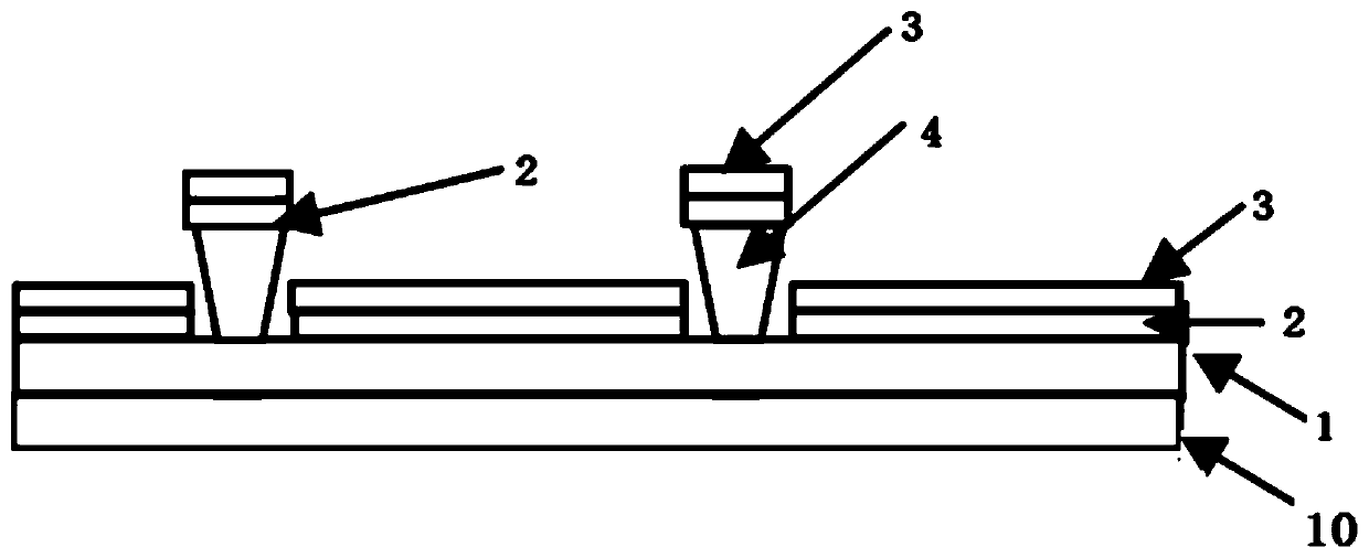
[0055] S1. A first electrode material layer is prepared on the substrate, and the first electrode material layer is patterned to form a plurality of first electrode units 1;
[0056] S2, on the first electrode unit 1, make spacers 4 arranged in parallel at intervals and arranged perpendicular to the direction of the first electrode unit 1;
[0057] S3, on the basis of step S2, fabricate the luminescent material layer 2 and the second electrode layer 3 by evaporation, and package.
[0058] When the insulating material layer 5 is provided in the first patterned area, S11 is also included between the step S1 and the step S2: an insulating material layer is prepared in the first patterned area on the basis of the step S1.
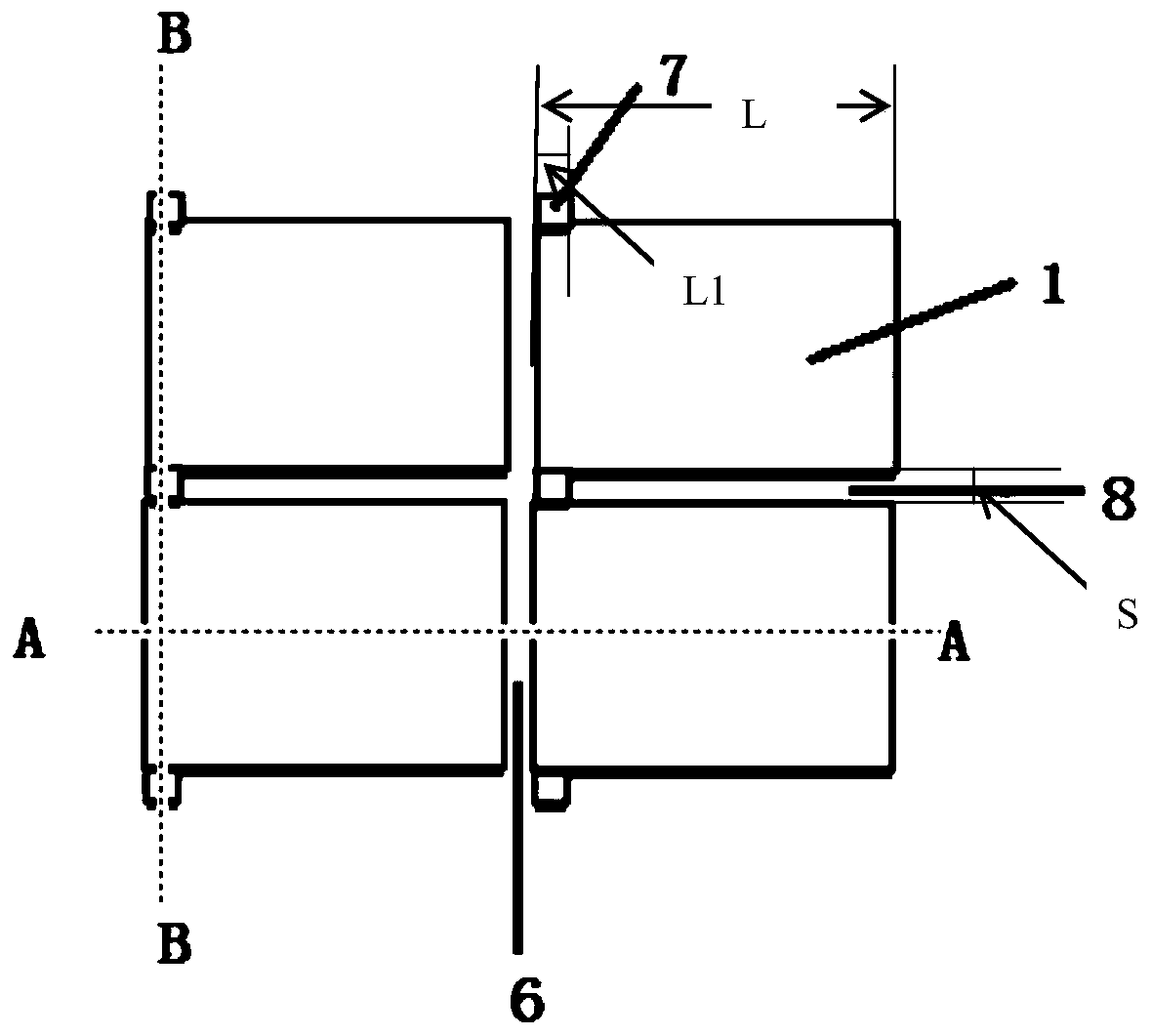
[0059] As another implementation, such as Figure 3 to Figure 10 As shown, a part of the first electrode unit 1 below the isolation column 4 is patterned into a secon...
Embodiment 1
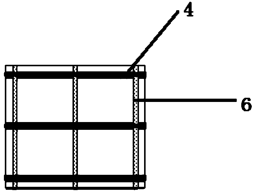
[0073] Device 1: as figure 1 and figure 2 As shown, the OLED device with high stability provided by this embodiment includes a substrate and a first electrode material layer (ITO layer) arranged on the substrate, and the first electrode material layer is patterned in the longitudinal direction A plurality of first electrode units 1, between the adjacent first electrode units 1 is the first patterned area 6 (that is, the longitudinal patterned area in the figure), and the horizontal direction on the first electrode unit 1 is provided with isolation Pillar 4 , the isolation post 4 is arranged in contact with the first electrode unit 1 . The first patterned area 6 is provided with an insulating material layer 5 . The insulating material layer 5 and the isolation column 4 are made of conventional insulating material layer phenolic resin.
[0074] Device 2: The structure is the same as that of device 1, wherein the insulating material layer 5 is an inorganic material layer such...
Embodiment 2
[0086] Device 3: No insulating material layer is provided under the isolation pillars and in the first patterned region. The preparation method of the device 3 does not include step S11.
[0087] In this embodiment, no insulating material layer is provided in the first patterned region 6 , and no insulating material layer is provided between the isolation post 4 and the first electrode unit 1 , so the path of moisture penetration can be reduced. In order to reduce the risk of short circuit caused by not providing an insulating material layer, the thickness of the luminescent material layer 2 is 300 nm to prevent leakage current at the edge of the first electrode unit, and the second electrode layer 3 is deposited on the luminescent material layer 2 . Unless otherwise specified, the material and thickness of each layer are the same as those of device 1.
[0088] Evaporate 200nm thick N,N-di(naphthalene-1-yl)-N,N'-diphenyl-benzidine (NPB) as hole transport layer; 9,10-di(2-nap...
PUM
 Abstract
Description
Claims
Application Information
 - R&D
- Intellectual Property
- Life Sciences
- Materials
- Tech Scout
- Unparalleled Data Quality
- Higher Quality Content
- 60% Fewer Hallucinations
Browse by: Latest US Patents, China's latest patents, Technical Efficacy Thesaurus, Application Domain, Technology Topic, Popular Technical Reports.
© 2025 PatSnap. All rights reserved.Legal|Privacy policy|Modern Slavery Act Transparency Statement|Sitemap|About US| Contact US: help@patsnap.com