Flexible display substrate, manufacturing method thereof and display device

A flexible display and display device technology, which is applied in the directions of identification devices, final product manufacturing, sustainable manufacturing/processing, etc., can solve problems such as separation of film layers, breakage of signal lines in wiring layers, poor process of flexible display substrates, etc., to achieve The effect of avoiding breakage and reducing the probability of defective workmanship

Active Publication Date: 2019-06-14
BOE TECH GRP CO LTD
View PDF15 Cites 14 Cited by
  • Summary
  • Abstract
  • Description
  • Claims
  • Application Information

AI Technical Summary

Problems solved by technology

[0004] However, the flexible display substrate includes a plurality of film layers stacked, the plurality of film layers include wiring layers, and the plurality of film layers are partially located in the bending area, and the binding area is bent to the side where the non-display surface is located. During the process, the part of the multiple film layers located in the bending area is prone to film layer separation, resulting in breakage of the signal lines of the wiring layer, and poor process of the flexible display substrate.

Method used


Image

  • Flexible display substrate, manufacturing method thereof and display device
  • Flexible display substrate, manufacturing method thereof and display device
  • Flexible display substrate, manufacturing method thereof and display device

Examples


Embodiment Construction

[0037] In order to make the purpose, technical solutions, and advantages of the application more clear, the application will be further described in detail below in conjunction with the accompanying drawings. Obviously, the described embodiments are only a part of the embodiments of the application, rather than all the embodiments. . Based on the embodiments in this application, all other embodiments obtained by those of ordinary skill in the art without creative work shall fall within the protection scope of this application.

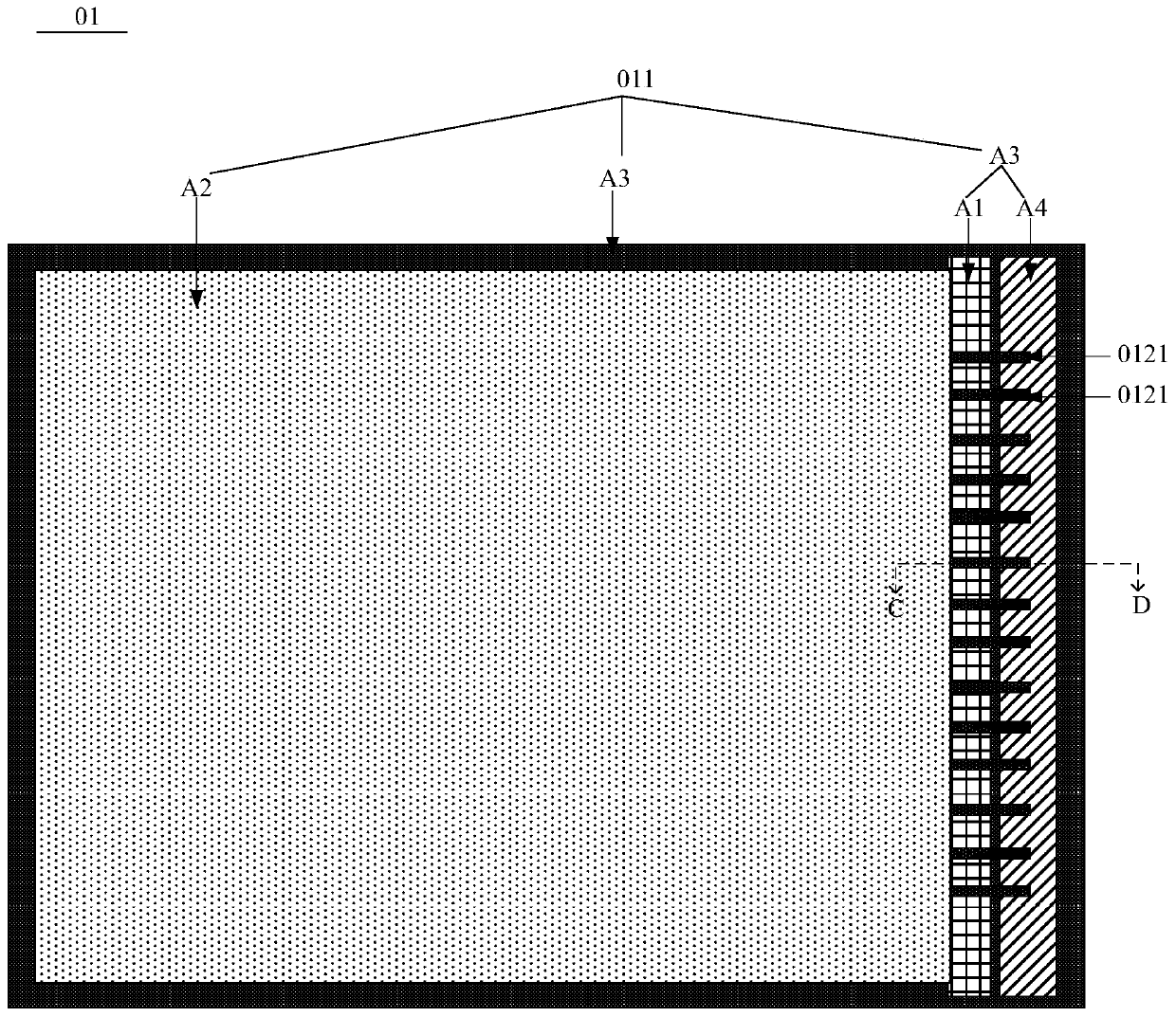
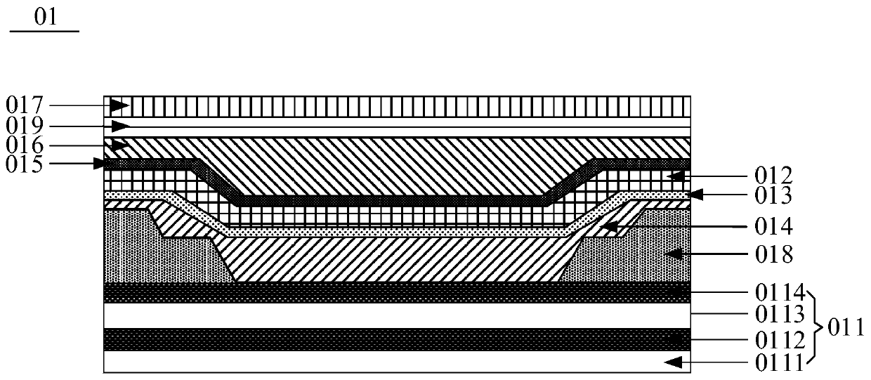
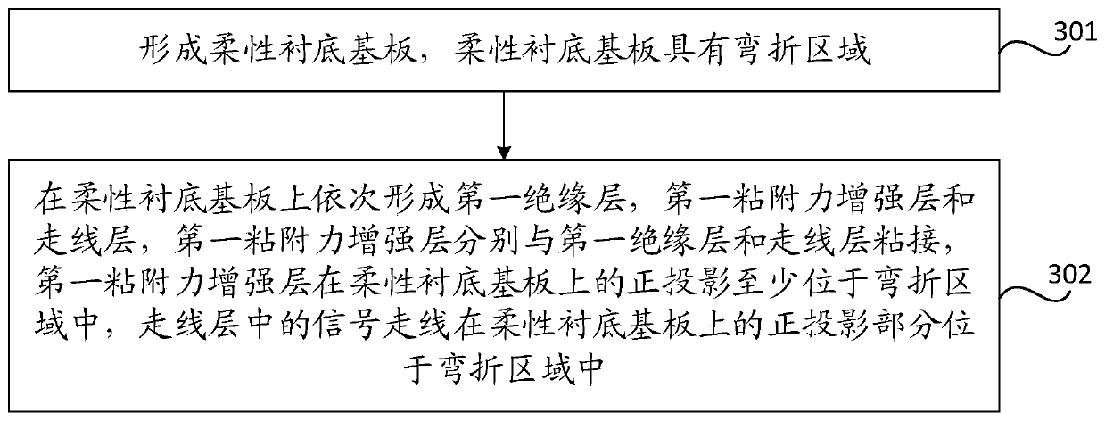
[0038] The flexible display substrate is known for its thin thickness and bendable performance. The flexible display substrate has a display surface and a non-display surface. The display surface has a display area and a non-display area. The non-display area usually includes a binding area. The area is used to bind the IC to the flexible display substrate. Usually, the binding area can be bent to the side where the non-display surface is located to achie...


PUM


Abstract

The invention relates to a flexible display substrate, a manufacturing method thereof and a display device, and belongs to the technical field of display. The flexible display substrate comprises: a flexible substrate, a routing layer, a first adhesion enhancement layer and a first insulating layer, wherein the routing layer, the first adhesion enhancement layer and the first insulating layer arelaminated on the flexible substrate; the first insulating layer is positioned on one side of the routing layer; the first adhesion enhancement layer is positioned between the first insulating layer and the routing layer; the first adhesion enhancement layer is respectively bonded with the first insulating layer and the routing layer; the flexible substrate is provided with a bending area; an orthographic projection of the first adhesion enhancement layer is at least positioned in the bending area of the flexible substrate; the orthographic projection of a signal routing in the routing layer ispartially positioned in the bending area of the flexible substrate; the first adhesion enhancement layer is used for enhancing the adhesion between the routing layer and the first insulating layer. The flexible display substrate is used for preventing signal wiring of the routing layer of the flexible display substrate from being broken.

Description

Technical field [0001] This application relates to the field of display technology, in particular to a flexible display substrate, a manufacturing method thereof, and a display device. Background technique [0002] With the development of display technology, display devices have gradually developed toward a narrow frame or even no frame. Currently, display devices with narrow bezels are mainly flexible display devices. [0003] The flexible display device includes a flexible display substrate. The flexible display substrate has a display surface and a non-display surface. The display surface has a display area and a non-display area. The non-display area includes an integrated circuit (English: Integrated Circuit; abbreviation: IC) and The binding area bound to the flexible display substrate can be bent to the side of the non-display surface to achieve a narrow or no border of the display device. When the binding area is bent to the side of the non-display surface, the non-display...

Claims


Application Information

Patent Timeline
Patent Type & Authority Applications(China)
IPC IPC(8): G09F9/30
CPCG09F9/30Y02E10/549Y02P70/50H10K59/12H10K77/111H10K2102/311H10K59/131H10K71/00H10K71/80H10K59/1201
Inventor 刘陆刘运进周伟峰
Owner BOE TECH GRP CO LTD
Why Eureka
Try Eureka