Semiconductor device and method of forming the same

A semiconductor and device technology, applied in the field of semiconductor devices and their formation, can solve problems such as performance to be improved, and achieve the effects of enhancing isolation performance, avoiding loss, and improving isolation performance

Active Publication Date: 2022-02-15
SEMICON MFG INT (SHANGHAI) CORP +1
View PDF20 Cites 0 Cited by
  • Summary
  • Abstract
  • Description
  • Claims
  • Application Information

AI Technical Summary

Problems solved by technology

[0004] However, the performance of semiconductor devices composed of fin field effect transistors in the prior art needs to be improved

Method used


Image

  • Semiconductor device and method of forming the same
  • Semiconductor device and method of forming the same
  • Semiconductor device and method of forming the same

Examples


Embodiment Construction

[0035] As mentioned in the background, semiconductor devices formed in the prior art have poor performance.

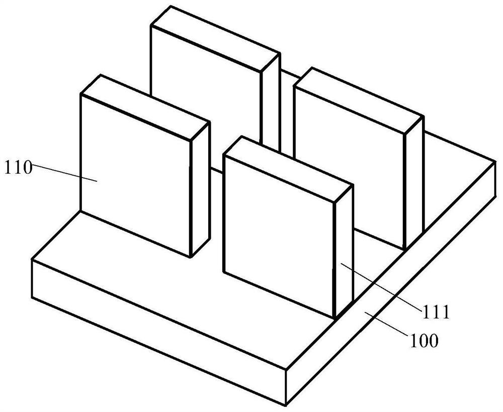
[0036] Figure 1 to Figure 5 It is a structural schematic diagram of the formation process of a semiconductor device.

[0037] refer to figure 1 , provide a semiconductor substrate 100, the semiconductor substrate 100 has a first fin 110 and a second fin 111, the extension direction of the first fin 110 and the second fin 111 is parallel, the first fin 110 and the second fin The semiconductor substrate 100 between the two fins 111 is an isolation region.

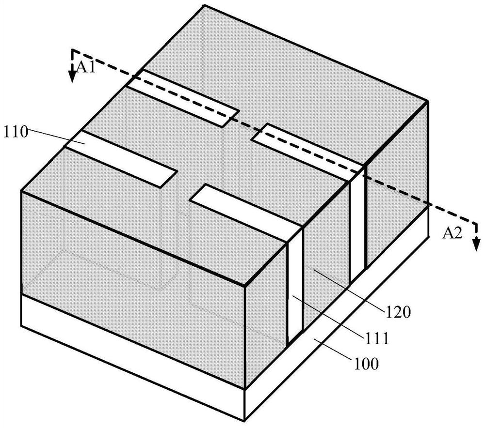
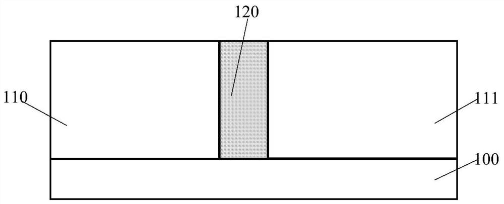
[0038] combined reference figure 2 and image 3 , image 3 for along figure 2 In the cross-sectional view of cutting line A1 - A2 , an isolation structure film 120 covering sidewalls of the first fin 110 and the second fin 111 is formed on the semiconductor substrate 100 .

[0039] refer to Figure 4 , Figure 4 for in image 3 Based on the schematic diagram formed, a mask layer 130 is formed on the isolati...


PUM

PropertyMeasurementUnit
thicknessaaaaaaaaaa

Abstract

A semiconductor device and a method for forming the same, wherein the method includes: providing a semiconductor substrate with initial fins on the semiconductor substrate; forming a gate structure material layer on the semiconductor substrate and the initial fins, the gate The top surface of the pole structure material layer is higher than the top surface of the initial fin; a groove is formed in the gate structure material layer and the initial fin, and the groove is along a direction perpendicular to the extending direction of the initial fin and parallel to the semiconductor substrate. The direction of the bottom surface runs through the initial fin so that the initial fin forms a fin; an isolation layer is formed in the groove, the top surface of the isolation layer is higher than the top surface of the fin; and the gate structure material is etched layer, so that the gate structure material layer forms a gate structure on both sides of the isolation layer, the gate structure straddles the fin and covers part of the top surface and part of the sidewall surface of the fin. The method improves the isolation performance of the semiconductor device.

Description

technical field [0001] The invention relates to the field of semiconductor manufacturing, in particular to a semiconductor device and a forming method thereof. Background technique [0002] MOS (Metal-Oxide-Semiconductor) transistors are one of the most important components in modern integrated circuits. The basic structure of the MOS transistor includes: a semiconductor substrate; a gate structure located on the surface of the semiconductor substrate, and the gate structure includes: a gate dielectric layer located on the surface of the semiconductor substrate and a gate electrode layer located on the surface of the gate dielectric layer; The source and drain doped regions in the semiconductor substrate on both sides of the pole structure. [0003] With the development of semiconductor technology, the ability of the traditional planar MOS transistor to control the channel current becomes weaker, resulting in serious leakage current. Fin Field Effect Transistor (Fin FET) i...

Claims


Application Information

Patent Timeline
Patent Type & Authority Patents(China)
IPC IPC(8): H01L21/336H01L29/06H01L29/78
CPCH01L21/76232H01L21/31116H01L21/3065H01L21/32137H01L21/823431H01L27/0886H01L29/66795H01L21/32135H01L21/28008H01L21/823481H01L21/76224H01L21/823821H01L29/66545H01L29/785H01L29/6656H01L27/0924
Inventor 周飞
Owner SEMICON MFG INT (SHANGHAI) CORP
Why Eureka
Try Eureka