An anti-cracking circuit module and a design method of the anti-cracking circuit module

A technology of circuit modules and design methods, applied in the field of chip security design, can solve problems such as incorrect reverse analysis, hanging metal wires, and reducing the ability of chips to prevent cracking, and achieve the effect of simple design and easy implementation

Pending Publication Date: 2019-05-31
BEIJING CELLIX REVEALING TECH
View PDF1 Cites 2 Cited by
  • Summary
  • Abstract
  • Description
  • Claims
  • Application Information

AI Technical Summary

Problems solved by technology

[0005] Among them, patent 201610530462.3 involves a chip design method to improve the anti-cracking ability of the chip. Although the patent also improves the anti-cracking ability of the chip by designing multiple versions of layout data, the metal wires and connections of different layout data in this patent The holes are all likely to change, which leads to a situation, that is, in the reverse analysis, if the connection holes are different, some metal lines will be suspended, and it is easy to find that the reverse analysis is incorrect, which reduces the chip's defense. ability to crack
like Figure 13 ~ Figure 15 shown, where Figure 13 It is a layout structure of a circuit diagram, Figure 14 is another layout structure of the circuit diagram, Figure 15 It is a layout structure obtained by mixing a layer of metal of the first layout structure and a layer of metal of the second layout structure. Figure 15 It can be seen that because the positions of the connection holes of the two structures are different, there will be a situation where the metal line is suspended

Method used


Image

  • An anti-cracking circuit module and a design method of the anti-cracking circuit module
  • An anti-cracking circuit module and a design method of the anti-cracking circuit module
  • An anti-cracking circuit module and a design method of the anti-cracking circuit module

Examples


Embodiment 1

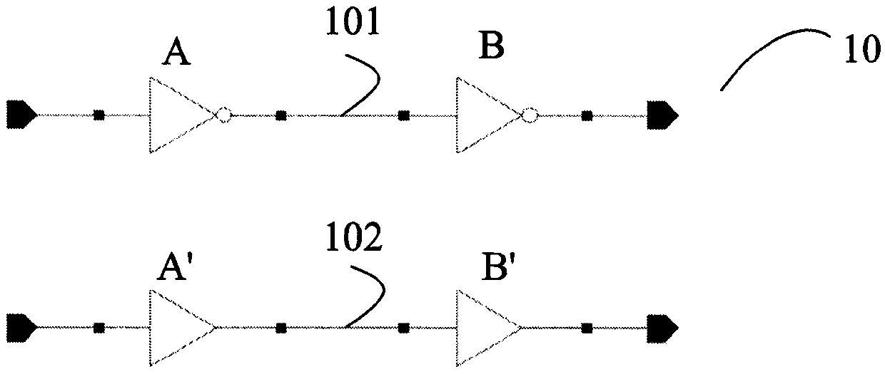
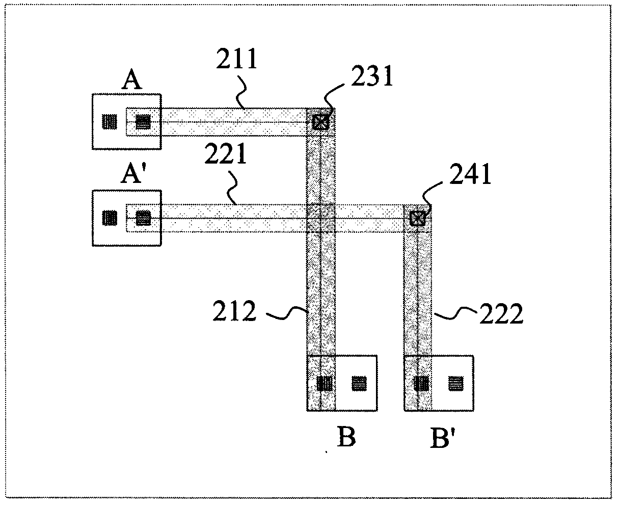
[0043] figure 1 is the circuit schematic diagram of the first embodiment, figure 2 for figure 1 The first layout form of the circuit diagram, image 3 for figure 1 The second layout form of the circuit diagram, Figure 4 for mixing figure 2 and image 3 The layout structure obtained by the different levels of the two layouts, Figure 5 By Figure 4 The circuit schematic diagram introduced by figure 1 and Figure 5 It can be seen that by mixing different layers of different layouts, the circuit schematic diagram will change, and the reverse analysis will fail. The unit in the following is just a generalization, not only referring to an inverter, but also referring to a transistor or a device. For the convenience of analysis, it can also refer to a circuit module, as long as it is within the scope of the present invention, it belongs to the protection to be protected Content.

[0044] Such as figure 1 As shown, the circuit Figure 10It includes 4 units, A, A'...

Embodiment 1

[0051] Another modified example of embodiment 1

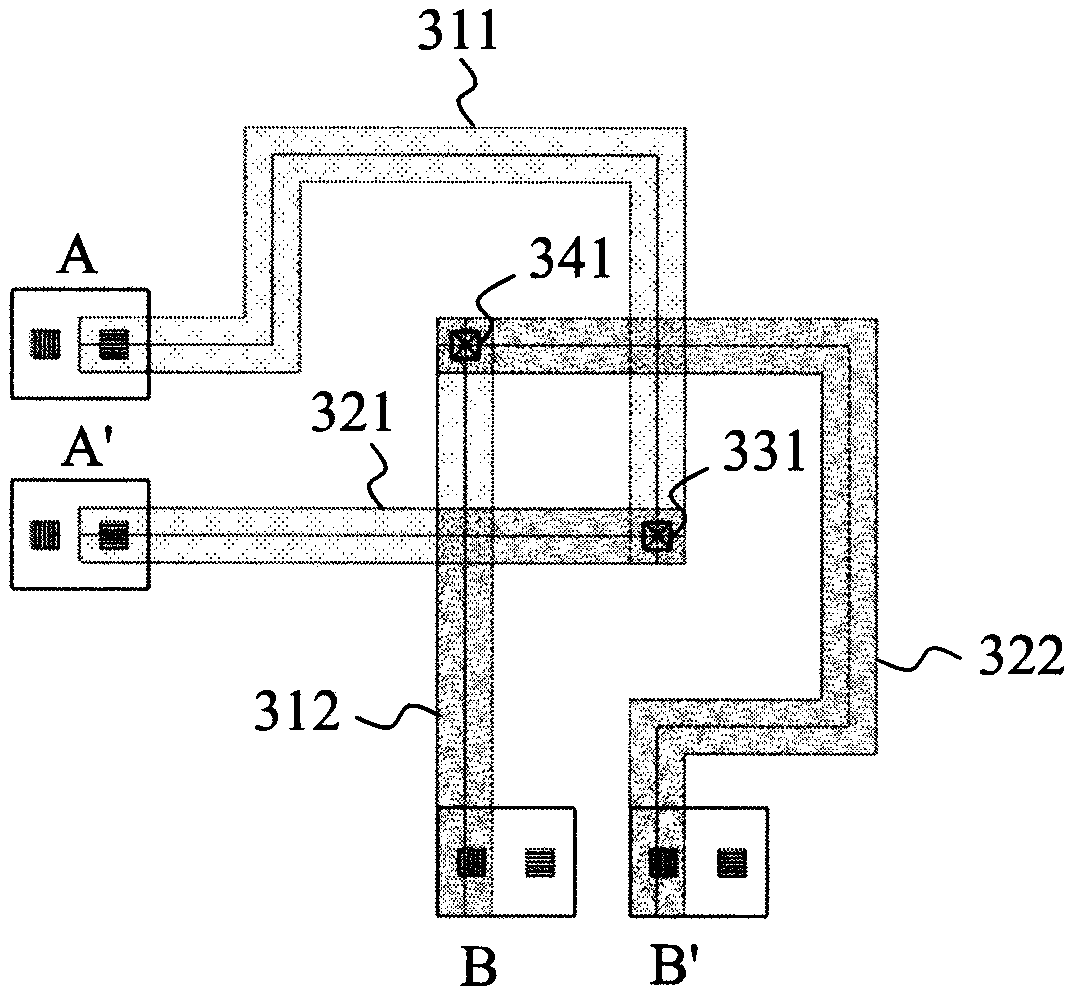
[0052] Figure 6 yes figure 1 The third layout form of the circuit diagram, Figure 7 for mixing figure 2 Metal layer 1 and Figure 6 The layout structure obtained by the reverse analysis of the chip with different levels of the two layouts of the metal layer 2, Figure 8 yes Figure 7 The circuit schematic diagram derived from the layout structure, by figure 1 and Figure 8 It can be seen that by mixing different layers of different layouts, the circuit schematic diagram will change, and the reverse analysis will fail.

[0053] Figure 6 It is another design scheme of the layout structure of the circuit 1. The layout of cells A, A', B, B' is as follows Figure 6 As shown, the output terminal of unit A is connected to the metal line 611, the metal line 611 is formed in the metal layer 1, the metal line 611 is connected to the metal line 612 through the connection hole 631, the metal line 612 is formed in the metal ...


PUM


Abstract

The invention discloses an anti-cracking circuit module and a design method of the anti-cracking circuit module, which can improve the anti-cracking capability of a chip and reduce the success rate ofreverse engineering to the minimum. The anti-cracking circuit module comprises at least two different layout structures. wherein the at least two different layout structures have the same circuit structure and the same metal layer number, each layout structure at least comprises two metal layers, the positions of the connecting holes of each layout structure are the same, and at least one layer of metal wires connected through the connecting holes are different. When a cracker adopts a plurality of chips with different layout structures to carry out layer-by-layer anatomical photographing, the obtained layout data is layout data formed by combining different layout structures, namely wrong layout data, and then a circuit structure diagram extracted according to the images is different from an originally designed circuit structure diagram, so that the anti-cracking capability of the chip is improved.

Description

technical field [0001] The invention belongs to the field of chip security design, and in particular relates to an anti-cracking circuit module and a design method of the anti-cracking circuit module. Background technique [0002] In the field of chip security design, an important protection goal is to prevent cracking, that is, to prevent crackers from obtaining the chip circuit structure, and obtaining the chip circuit structure requires reverse engineering of the chip. Reverse engineering includes package dissection and die analysis of the chip. Package dissection is very simple, while die analysis is more complicated, including multiple links. The first link is to obtain the layered photos of the die, and the subsequent link is to extract the circuit according to the photos. And analysis, so the key point of reverse engineering is to get the layered photos of the die. However, in order to obtain the photo of the lower layer except the top layer, it is necessary to grind...

Claims


Application Information

Patent Timeline
Patent Type & Authority Applications(China)
IPC IPC(8): G06F21/75G06F17/50
Inventor 张崇茜史可鑫丁仲
Owner BEIJING CELLIX REVEALING TECH
Why Eureka
Try Eureka