A design method of a cracker-proof chip and a cracker-proof chip

A design method and anti-cracking technology, applied in the protection of internal/peripheral computer components, etc., can solve the problem of safe design without reverse engineering, and achieve the effect of simple design and easy implementation

Pending Publication Date: 2019-02-05
BEIJING CELLIX REVEALING TECH
View PDF0 Cites 1 Cited by
  • Summary
  • Abstract
  • Description
  • Claims
  • Application Information

AI Technical Summary

Problems solved by technology

[0004] The existing chip security design methods are all realized by increasing the degree of confidentiality, such as encrypting the communication process, or adding a maze covering layer on the die, etc., and have not designed security for the characteristics of reverse engineering.

Method used


Image

  • A design method of a cracker-proof chip and a cracker-proof chip
  • A design method of a cracker-proof chip and a cracker-proof chip
  • A design method of a cracker-proof chip and a cracker-proof chip

Examples


Embodiment Construction

[0050] The technical solutions in the embodiments of the present invention will be clearly and completely described below in conjunction with the drawings in the embodiments of the present invention. The described embodiments are only part of the embodiments of the present invention, not all of them. Based on the embodiments of the present invention, all other embodiments obtained by persons of ordinary skill in the art without performing creative work belong to the protection scope of the present invention.

[0051] It should be noted that, in the case of no conflict, the embodiments of the present invention and the features in the embodiments can be combined with each other.

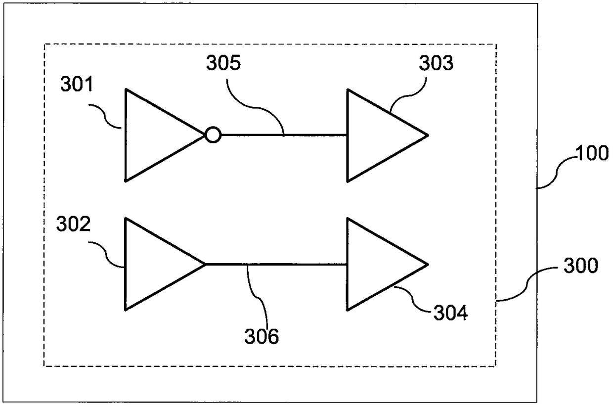
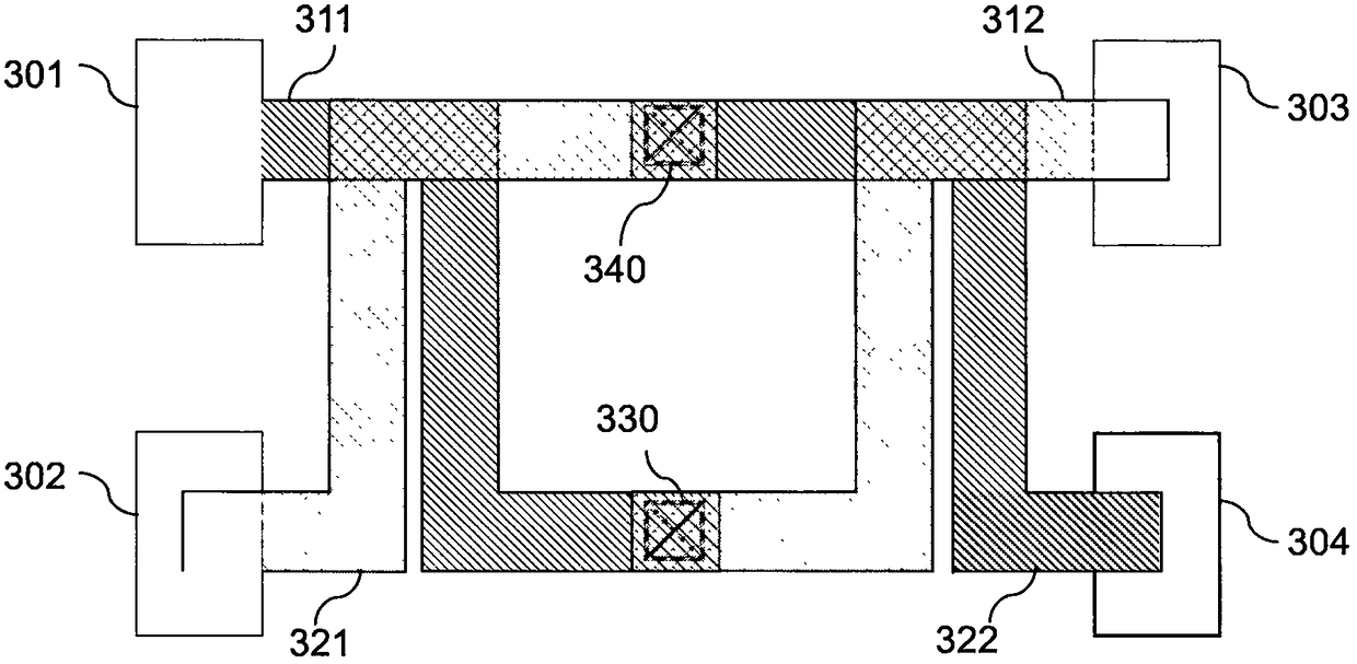
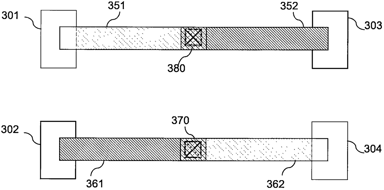
[0052] In order to solve the problem that the chip is cracked, a design method of an anti-cracking chip is proposed, such as Figure 19 shown, including the following steps:

[0053] Step S121, circuit structure design. Circuit design is the first step in the overall process of producing chips. Desi...


PUM


Abstract

The invention provides a design method of anti-cracking chip, At that time of chip design, A plurality of different layout data are designed according to the same circuit structure, and a plurality ofdifferent layout data are respectively made into corresponding mask templates, and these different types of mask templates are placed in the same exposure window for photolithography, so that the produced die will have different physical structures, but the circuit structure is the same. When encapsulated, encapsulate it into a package that looks the same. When multiple chips are used for layer-by-layer anatomical photography, the probability of obtaining each layer image of the same layout data is very low, and then the circuit structure diagram extracted from these images is different fromthe circuit structure diagram of the original design, so the anti-cracking ability of the chip is improved.

Description

technical field [0001] The invention belongs to the field of chip security design, and in particular relates to a design method of an anti-cracking chip and an anti-cracking chip. Background technique [0002] In the field of chip security design, an important protection goal is to prevent cracking, that is, to prevent crackers from obtaining the chip circuit structure, and obtaining the chip circuit structure requires reverse engineering of the chip. Reverse engineering includes package dissection and die analysis of the chip. Package dissection is very simple, while die analysis is more complicated, including multiple links. The first link is to obtain the layered photos of the die, and the subsequent link is to extract the circuit according to the photos. And analysis, so the key point of reverse engineering is to get the layered photos of the die. In order to obtain the lower layer photo except the top layer, it is necessary to grind or etch the die to remove the upper ...

Claims


Application Information

Patent Timeline
Patent Type & Authority Applications(China)
IPC IPC(8): G06F21/76
CPCG06F21/76
Inventor 熊伟张军
Owner BEIJING CELLIX REVEALING TECH
Why Eureka
Try Eureka