A kind of image sensor and preparation method thereof
An image sensor and photosensitive device technology, applied in the semiconductor field, can solve the problems of increasing the difficulty of image sensor preparation and not being suitable for silicon thickness image sensors, etc., and achieve the effects of easy operation, improved absorption, and increased optical path
- Summary
- Abstract
- Description
- Claims
- Application Information
AI Technical Summary
Problems solved by technology
Method used
Image
Examples
Embodiment 1
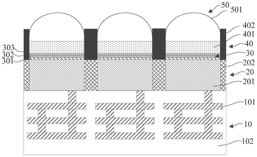
[0079] Refer to attached Figure 1-3 , this embodiment provides an image sensor, such as figure 1 As shown, the image sensor of this embodiment includes a metal interconnection layer 10 , a photosensitive device layer 20 , an optical path adjustment layer 30 , a filter layer 40 and a microlens array 50 .
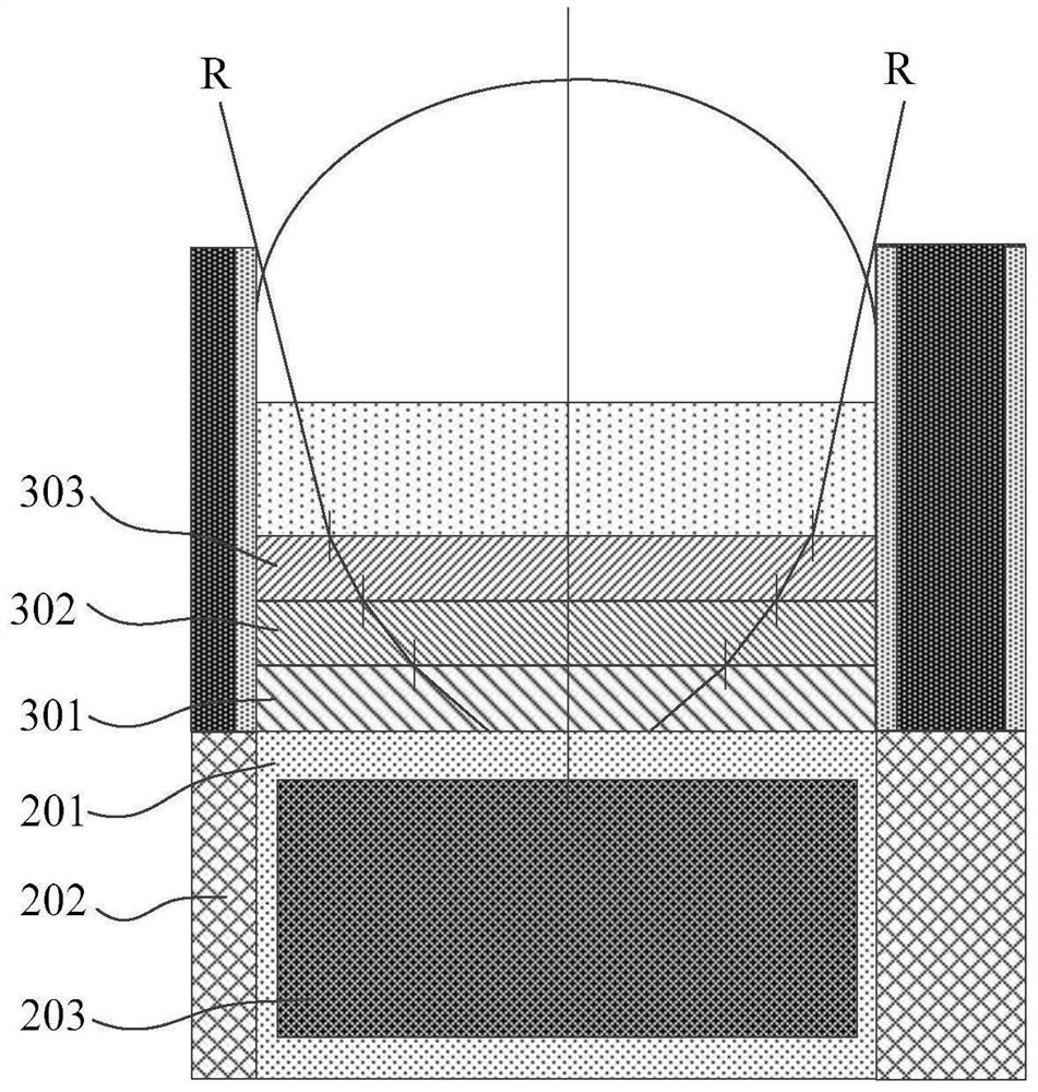
[0080] Such as figure 1 As shown, the photosensitive device layer 20 includes at least one photosensitive region 201 , and the photosensitive regions 201 are isolated by deep trench isolation structures 202 . In a preferred embodiment of this embodiment, at least one photosensitive area 201 may be distributed in an array.
[0081] Such as image 3 As shown, in a further embodiment of this embodiment, the photosensitive region 201 further includes a PN junction structure 203 .
[0082] The metal interconnection layer 10 is located on the lower surface of the photosensitive device layer 20 , and the metal interconnection layer 10 includes at least one metal interconnection...
Embodiment 2
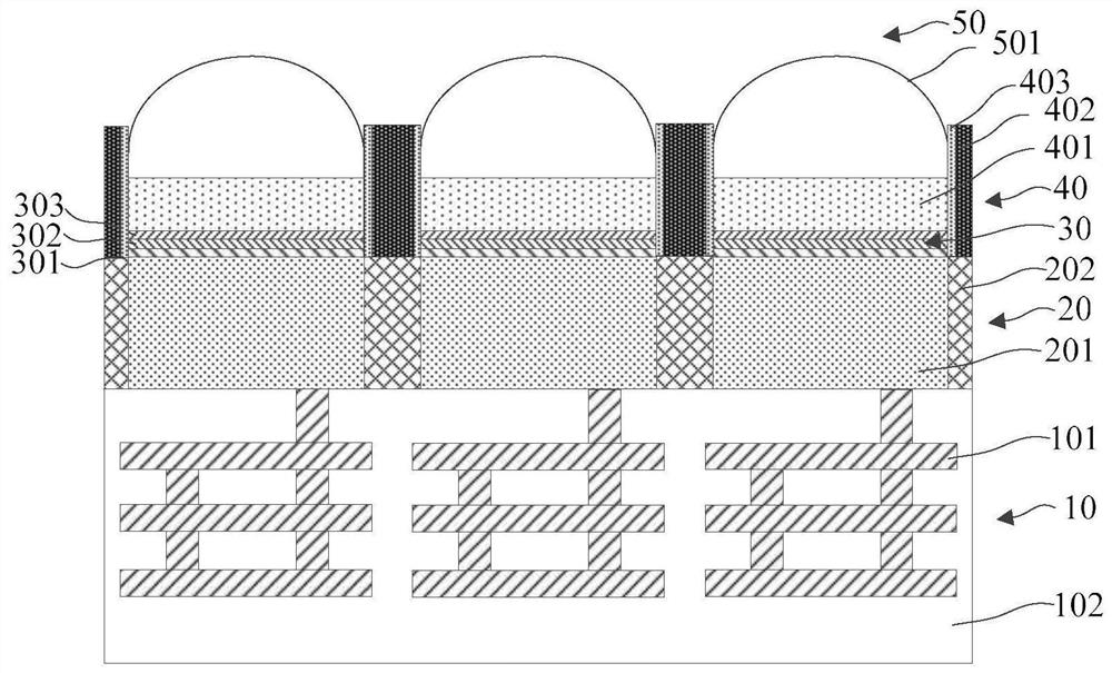
[0093] This embodiment also provides an image sensor. The similarities between this embodiment and Embodiment 1 will not be repeated, and the difference lies in:
[0094] Such as figure 2 As shown, in the image sensor of this embodiment, at least one optical filter 401 further includes a peripheral oxide 403, and the peripheral oxide 403 is deposited around the metal grid 402 and covers at least one side of the metal grid 402 side wall. The peripheral oxide 403 can protect the filter 401 from metal contamination that may be caused by the metal grid.
Embodiment 3
[0096] This embodiment provides a method for preparing an image sensor, such as Figure 6 Shown, this preparation method comprises the steps:
[0097] providing a semiconductor substrate including a photosensitive device layer;
[0098] Depositing multiple layers of transparent substances sequentially above the photosensitive device layer to form an optical path adjustment layer;
[0099] A filter is placed over a transparent substance to form a filter layer; wherein,
[0100] The photosensitive device layer includes at least one photosensitive area, and the multilayer transparent substances have different refractive indices.
[0101] refer to Figure 7-12 , and again refer to figure 1 and image 3 , the preparation method of the image sensor is described in detail.
[0102] Such as Figure 7 As shown, a semiconductor substrate including a photosensitive device layer 20 is provided, and the photosensitive device layer 20 includes at least one photosensitive region 201, ...
PUM
 Abstract
Description
Claims
Application Information
 - R&D
- Intellectual Property
- Life Sciences
- Materials
- Tech Scout
- Unparalleled Data Quality
- Higher Quality Content
- 60% Fewer Hallucinations
Browse by: Latest US Patents, China's latest patents, Technical Efficacy Thesaurus, Application Domain, Technology Topic, Popular Technical Reports.
© 2025 PatSnap. All rights reserved.Legal|Privacy policy|Modern Slavery Act Transparency Statement|Sitemap|About US| Contact US: help@patsnap.com


