Eureka AIR delivers breakthrough ideas for toughest innovation challenges, trusted by R&D personnel around the world.

Three-dimensional storage device and fabrication method thereof

A manufacturing method and memory technology, applied in the direction of electric solid-state devices, semiconductor devices, electrical components, etc., can solve the problems of memory space occupied by support columns, larger memory volume, memory leakage, etc., to reduce manufacturing costs, improve integration and performance, area reduction effect

Inactive Publication Date: 2019-05-14
YANGTZE MEMORY TECH CO LTD
View PDF2 Cites 23 Cited by
  • Summary
  • Abstract
  • Description
  • Claims
  • Application Information

AI Technical Summary

Problems solved by technology

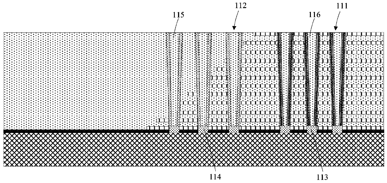
[0006] In view of the above-mentioned shortcomings of the prior art, the purpose of the present invention is to provide a three-dimensional memory and its manufacturing method, which is used to solve the problem that the bottom of the supporting pillars in the prior art is usually filled with conductive semiconductor material, which easily leads to leakage of the memory. , at the same time, the support column needs to occupy additional storage space, resulting in the problem that the volume of the storage becomes larger

Method used


Image

  • Three-dimensional storage device and fabrication method thereof
  • Three-dimensional storage device and fabrication method thereof
  • Three-dimensional storage device and fabrication method thereof

Examples


Embodiment Construction

[0080] Embodiments of the present invention are described below through specific examples, and those skilled in the art can easily understand other advantages and effects of the present invention from the content disclosed in this specification. The present invention can also be implemented or applied through other different specific implementation modes, and various modifications or changes can be made to the details in this specification based on different viewpoints and applications without departing from the spirit of the present invention.

[0081] For example, when describing the embodiments of the present invention in detail, for the convenience of explanation, the cross-sectional view showing the device structure will not be partially enlarged according to the general scale, and the schematic diagram is only an example, which should not limit the protection scope of the present invention. In addition, the three-dimensional space dimensions of length, width and depth sho...


PUM


Abstract

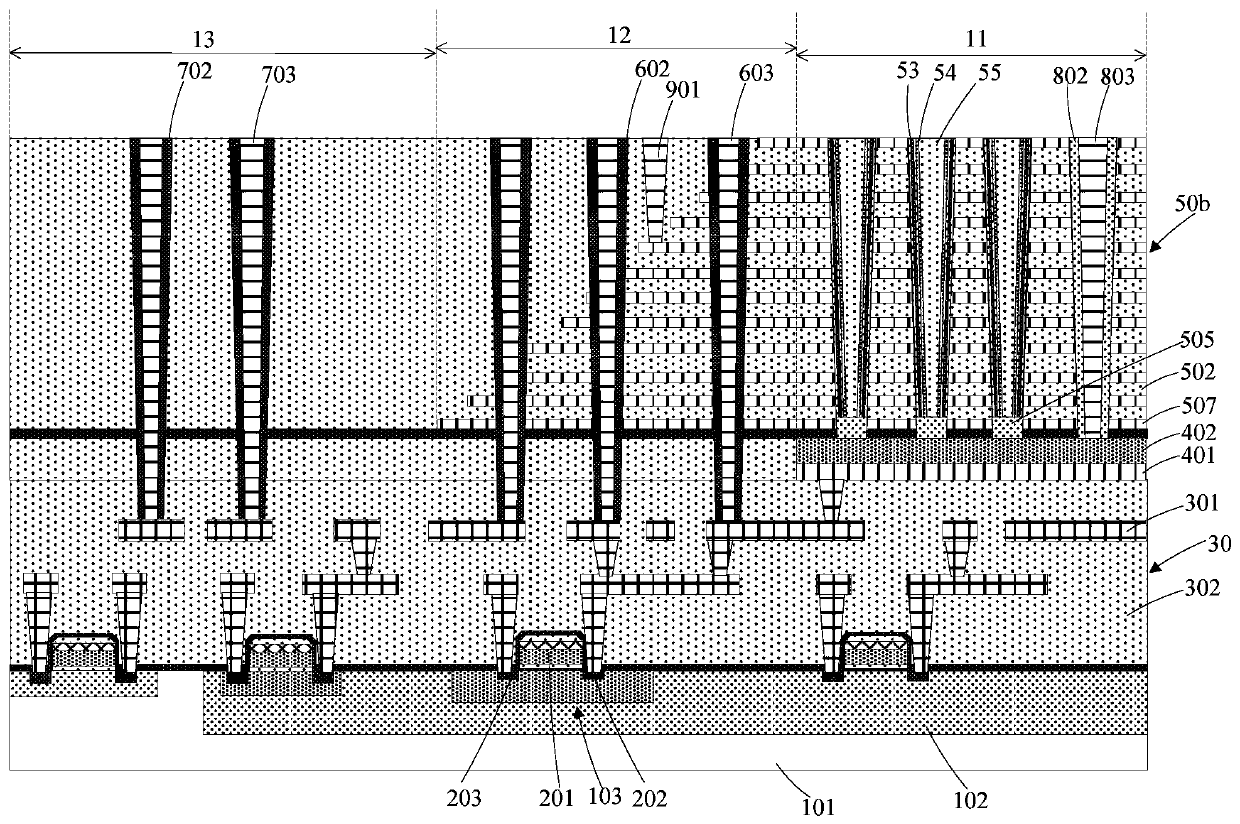
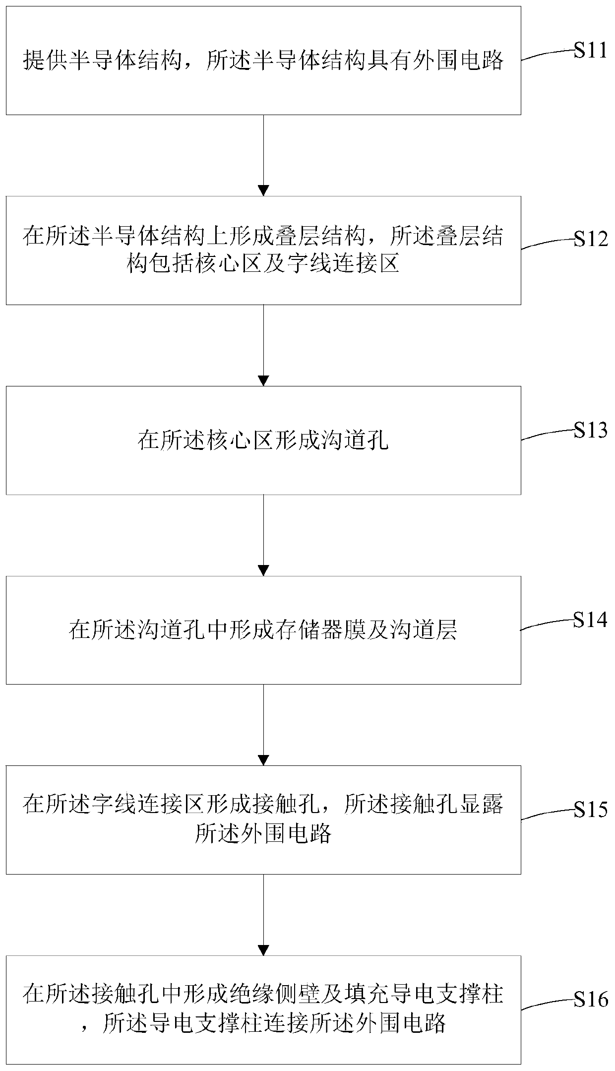
The invention relates to the field of semiconductor design and manufacturing, in particular to a three-dimensional storage device and a fabrication method thereof. The three-dimensional storage devicecomprises a semiconductor structure and a stack structure, wherein the semiconductor structure is provided with a peripheral circuit, the stack structure is arranged on the peripheral circuit and comprise a core region and a word line connection region, a channel hole is formed in the core region, a storage device film and a channel layer are formed in the channel hole, a contact hole is formed in the word line connection region and penetrates through the word line connection region, an insulation side wall and a conductive support post are formed in the contact hole, and the conductive support post is connected with the peripheral circuit. By the three-dimensional storage device, the integration and the performance of the three-dimensional storage device are improved; and meanwhile, short circuit or electric leakage of the device caused by filling of poly-silicon in the bottom of the contact hole can be prevented, and the electrical stability and the yield of the three-dimensional storage device are improved.

Description

technical field [0001] The invention belongs to the field of semiconductor design and manufacture, and in particular relates to a three-dimensional memory and a manufacturing method thereof. Background technique [0002] With the development of planar flash memory, the production process of semiconductors has made great progress. However, in recent years, the development of planar flash memory has encountered various challenges: physical limits, existing development technology limits, and storage electron density limits. In this context, in order to solve the difficulties encountered in planar flash memory and to pursue lower production costs per unit storage unit, a three-dimensional memory structure emerged as the times require. The three-dimensional memory structure can make each memory die in the memory device have more numbers. memory unit. [0003] In non-volatile memory, such as NAND memory, one way to increase memory density is by using vertical memory arrays, that...

Claims


Application Information

Patent Timeline
Patent Type & Authority Applications(China)
IPC IPC(8): H01L27/11582H01L27/11575H01L27/11573H01L27/1157H10B43/27H10B43/35H10B43/40H10B43/50
Inventor 刘峻
Owner YANGTZE MEMORY TECH CO LTD
Why Eureka
Eureka Blog
Learn More