Optical fingerprint identification device
A fingerprint identification and optical technology, applied in the field of fingerprint identification, can solve problems that affect the reliability of fingerprint identification, light refraction and scattering, and affect the clarity of fingerprint imaging, etc., to achieve the effect of improving clarity, improving signal-to-noise, and improving reliability
- Summary
- Abstract
- Description
- Claims
- Application Information
AI Technical Summary
Problems solved by technology
Method used
Image
Examples
Embodiment 1
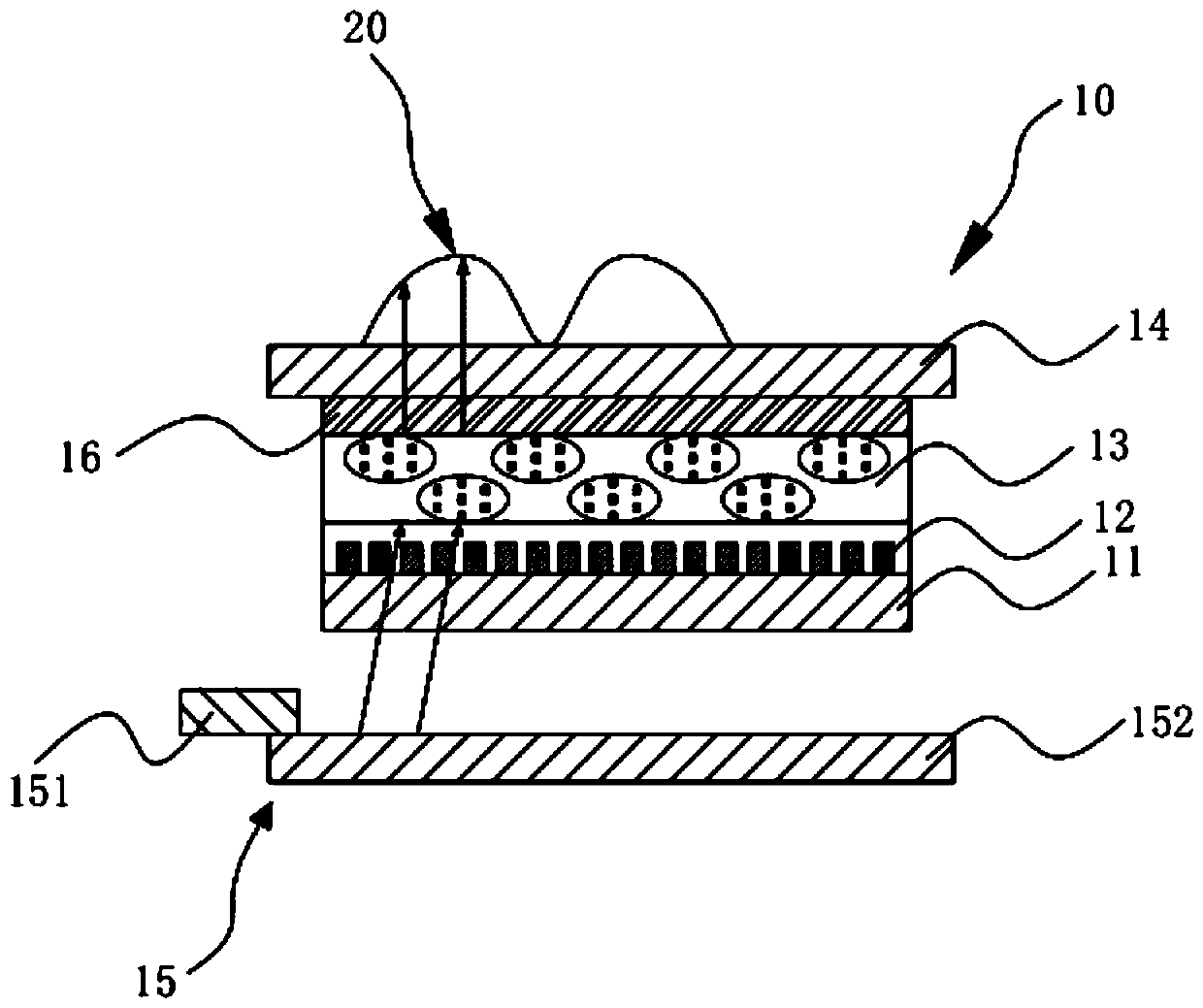
[0025] Such as figure 1 As shown, the present invention provides an optical fingerprint identification device 10, which includes a substrate 11, a photosensitive element 12, a collimating layer 13, a cover plate 14, and a backlight module 15.
[0026] Wherein, the photosensitive element 12 is disposed on the substrate 11, the cover plate 14 is disposed on the photosensitive element 12, and the cover plate 14 is located on the top layer of the fingerprint identification device 10 to encapsulate and protect The function of the device, the cover plate 14 is transparent glass, and the cover plate 14 is in contact with the fingerprint 20 of the human body.
[0027] The backlight module 15 is disposed on a side of the substrate 11 facing away from the photosensitive element 12, and the backlight module 15 provides a light source for optical fingerprint recognition.
[0028] The collimation layer 13 is formed by dispersing liquid crystals in solid organic polymers. The material of the colli...
Embodiment 2
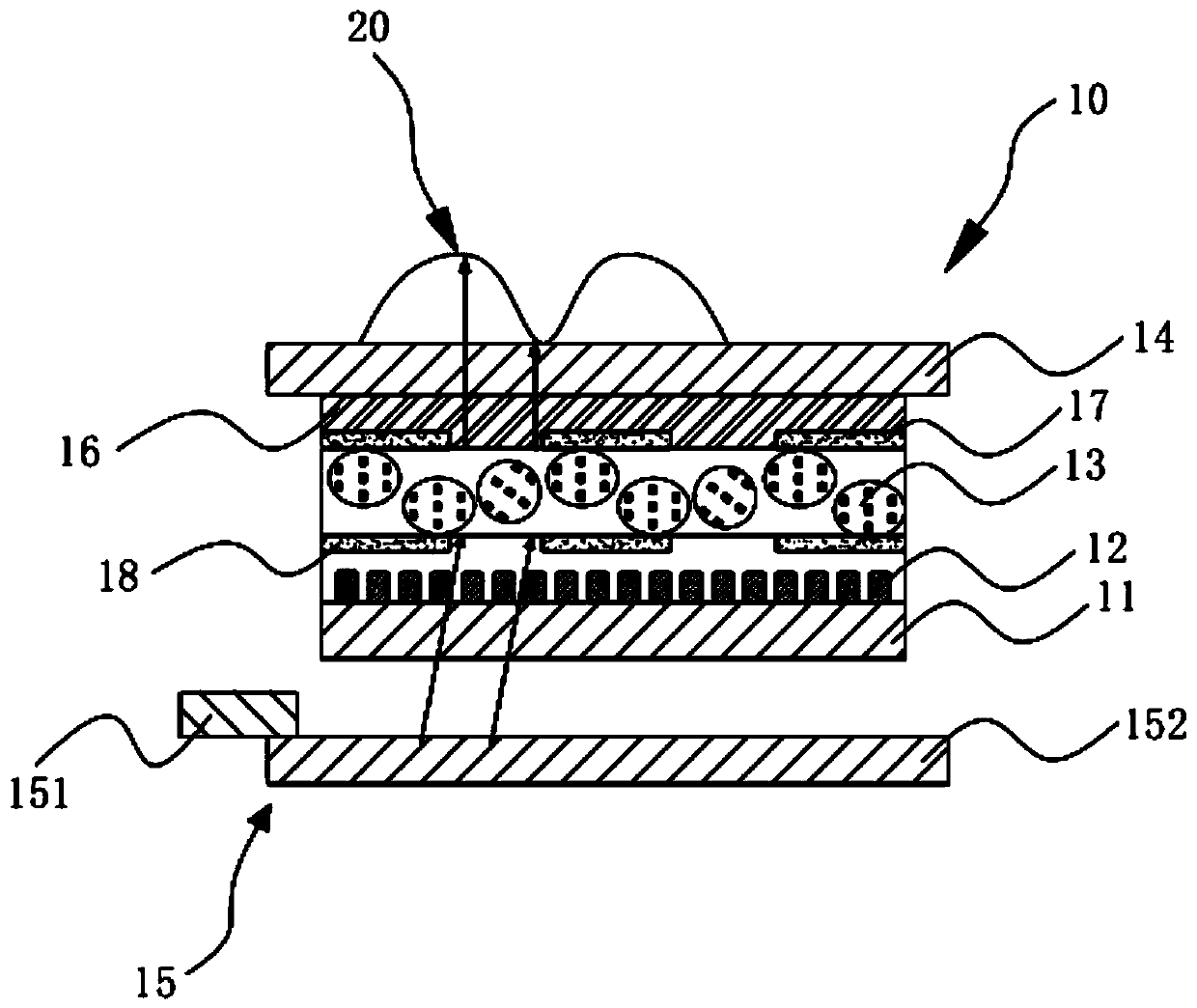
[0039] Such as figure 2 As shown, the difference from the first embodiment is that the two opposite surfaces of the collimation layer 13 are respectively provided with a first electrode layer 17 and a second electrode layer 18, and the first electrode layer 17 is provided on the collimation layer. 13 is a side surface (upper surface) away from the substrate 11, and the second electrode layer 18 is disposed on a side surface (lower surface) of the collimating layer 13 close to the substrate 11. The electrode patterns of the first electrode layer 17 and the second electrode layer 18 are the same and arranged correspondingly. The materials of the first electrode layer 17 and the second electrode layer 18 are both ITO (Indium tin oxide, indium oxide). tin).
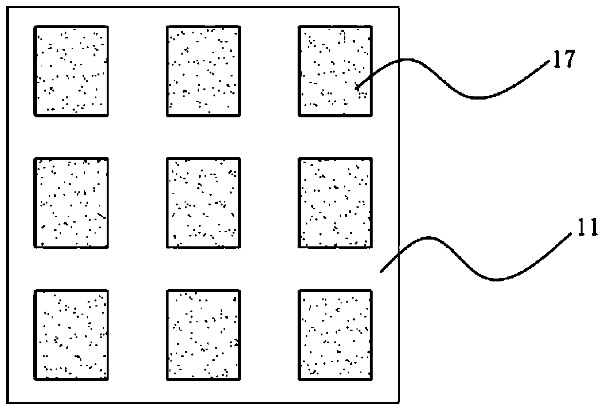
[0040] Such as image 3 As shown, the electrode pattern of the first electrode layer 17 is an array of small electrode blocks, the length and width of the electrode blocks can be 2-100 microns, the row spacing and column spacin...
Embodiment 3
[0043] Such as Figure 4 As shown, this embodiment provides an optical fingerprint identification device 30, which includes a substrate 31, a photosensitive element 32, a collimation layer 33, an OLED display layer 35, an adhesive layer 36, and a cover 34.
[0044] Wherein, the photosensitive element 33 is disposed on the substrate 31, the collimation layer 33 is disposed on the photosensitive element 32, the cover plate 34 is disposed on the collimation layer 33, and the OLED display The layer 35 is disposed between the collimating layer 33 and the cover plate 34.
[0045] The adhesive layer 36 is disposed on the cover plate 34 and the OLED display layer 35 for bonding the cover plate 34 and the OLED display layer 35.
[0046] The substrate 31 may be a flexible substrate, and the cover plate 34 is transparent glass for packaging and protecting the device and contacting the fingerprint 20 of the human body.
[0047] The collimation layer 35 is a PDLC film, the refractive index of the...
PUM
| Property | Measurement | Unit |
|---|---|---|
| thickness | aaaaa | aaaaa |
| width | aaaaa | aaaaa |
| transmittivity | aaaaa | aaaaa |
Abstract
Description
Claims
Application Information
 - R&D
- Intellectual Property
- Life Sciences
- Materials
- Tech Scout
- Unparalleled Data Quality
- Higher Quality Content
- 60% Fewer Hallucinations
Browse by: Latest US Patents, China's latest patents, Technical Efficacy Thesaurus, Application Domain, Technology Topic, Popular Technical Reports.
© 2025 PatSnap. All rights reserved.Legal|Privacy policy|Modern Slavery Act Transparency Statement|Sitemap|About US| Contact US: help@patsnap.com


