Semiconductor wafer precision cutting device

A cutting device and semiconductor technology, applied in semiconductor/solid-state device manufacturing, electrical components, circuits, etc., can solve the problems of semiconductor wafer scrapping, difficulty in replacing cutter heads, and reduced production, so as to improve cutting accuracy and avoid cutting failure , Improve the effect of cutting quality

Active Publication Date: 2019-03-26
JIANGSU NEPES SEMICON
View PDF5 Cites 0 Cited by
  • Summary
  • Abstract
  • Description
  • Claims
  • Application Information

AI Technical Summary

Problems solved by technology

[0003] At present, in the cutting technology on the market, laser cutting is mostly used. Although the cutting effect is good and the process is good, heat is generated, which is easy to cause wafer deformation. At the same time, the heat-affected zone is also easy to cause circuit rust, which in turn leads to the scrapping of semiconductor wafers. Due to the high environmental requirements for semiconductor wafer cutting, dust needs to be avoided. In addition, the cutting head is a vulnerable part. If it is not properly set, it will often lead to difficulty in replacing the cutting head and reduce production. At the same time, if the semiconductor wafer cutting process, Without stable fixation, semiconductor wafers will often be completely scrapped. Therefore, in view of the above status quo, it is urgent to develop a semiconductor wafer precision cutting device to overcome the shortcomings in current practical applications.

Method used


Image

  • Semiconductor wafer precision cutting device
  • Semiconductor wafer precision cutting device
  • Semiconductor wafer precision cutting device

Examples


Embodiment 1

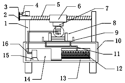
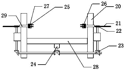
[0024] see Figure 1~3 , in an embodiment of the present invention, a semiconductor wafer precision cutting device includes a support rod 1, a fixing device 8, a fixing seat 10 and a cutter head 17, and the support rod 1 is provided on both sides of the top of the fixing seat 10, and the left side supports A first motor 4 is provided on the left side of the top of the rod 1, and the first motor 4 is bolted to the support rod 1, and the left output end of the first motor 4 is connected to the second gear 3, and the lower side of the second gear 3 A screw 5 bearing-connected to the support rod 1 is provided, the left end of the screw 5 is provided with a first gear 2, and the first gear 2 is meshed with the second gear 3, and the screw 5 is located between the two support rods 1 The outer side of the middle part is provided with a first fixed block 6, and the first fixed block 6 is threadedly connected with the screw mandrel 5, and the bottom of the first fixed block 6 is provid...

Embodiment 2

[0028] A cutting device includes the precise semiconductor wafer cutting device described in Embodiment 1.

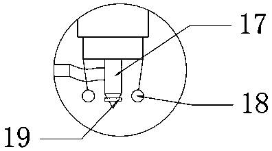
[0029] The semiconductor wafer precision cutting device can effectively remove the impurities generated after cutting by setting multi-layer filters, thereby ensuring the cleanness and recycling of the cutting fluid, avoiding the secondary pollution of the semiconductor wafer, and reducing the cutting fluid. The use cost also protects the environment. By setting the fixing device 8, the wafer can be effectively fixed, avoiding the cutting failure caused by the side slip of the wafer during the cutting process, and improving the cutting accuracy. The adjustment of the light source 18 The angle ranges from 0 to 90 degrees, so that the light source 18 can be completely and accurately aligned on the semiconductor wafer. By setting the light source sensor 19, the precision of cutting can be effectively improved and the cutting quality can be improved.

[0030] The working pr...


PUM


Abstract

The invention relates to the technical field of cutting equipment, in particular to a semiconductor wafer precision cutting device. The semiconductor wafer precision cutting device includes support rods, a fixing device, a fixed seat and a cutter head. The support rods are arranged on the two sides of the top of the fixed seat. A first motor is arranged on the left side of the top of the left support rod. A screw rod is arranged on the lower side of the first motor. A first fixing block is arranged on the outer side of the part of the screw rod between the two support rods. A telescopic rod isarranged at the bottom of the first fixing block. The cutter head is arranged at the bottom of the telescopic rod. Light sources are arranged on the two sides of the cutter head. A light source sensor is arranged at the lower end of the cutter head. The fixing device is arranged on the lower side of the cutter head. Through the setting of the fixing device, a wafer can be well fixed, cutting failure due to side slip of wafers in the cutting process is avoided, and the cutting accuracy is improved. Through the setting of the light source sensor, the precision of cutting can be improved, and the quality of cutting can be improved.

Description

technical field [0001] The invention relates to the technical field of cutting equipment, in particular to a semiconductor wafer precision cutting device. Background technique [0002] Wafer (Wafer) refers to the silicon wafer used in the production of silicon semiconductor integrated circuits. Because of its circular shape, it is called a wafer. In the production and application of semiconductors, wafer cutting is essential, and the cutting of semiconductor wafers The quality directly determines whether the semiconductor is qualified. [0003] At present, in the cutting technology on the market, laser cutting is mostly used. Although the cutting effect is good and the process is good, heat is generated, which is easy to cause wafer deformation. At the same time, the heat-affected zone is also easy to cause circuit rust, which in turn leads to the scrapping of semiconductor wafers. Due to the high environmental requirements for semiconductor wafer cutting, dust needs to be ...

Claims


Application Information

Patent Timeline
Patent Type & Authority Applications(China)
IPC IPC(8): H01L21/67H01L21/304
CPCH01L21/3043H01L21/67092
Inventor 杨雪松袁泉孙健陈业
Owner JIANGSU NEPES SEMICON
Why Eureka
Try Eureka