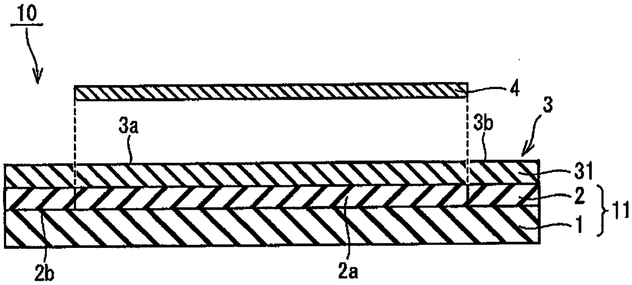
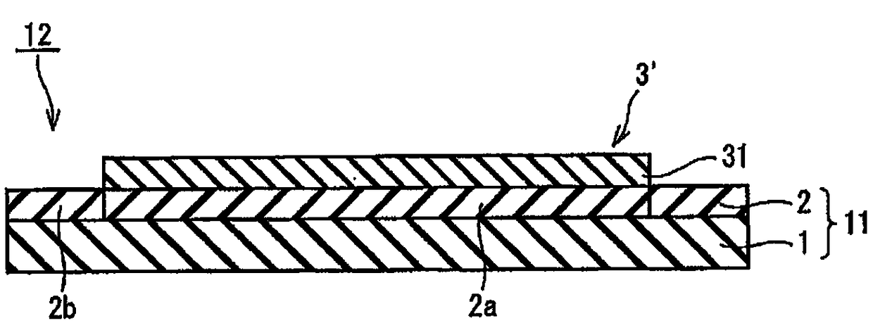
Heat bonding sheet, and heat bonding sheet with dicing tape
A technology for cutting tapes and sheets, used in conductive adhesives, inorganic adhesives, adhesive additives, etc., can solve problems such as thermal characteristics and reliability problems
- Summary
- Abstract
- Description
- Claims
- Application Information
AI Technical Summary
Problems solved by technology
Method used
Image

Examples
Embodiment 1~3 and comparative example 1
[0166] 100 parts by weight of a paste containing sinterable metal particles, 7 parts by weight of a pyrolytic binder shown in Table 1, and 45 parts by weight of an organic solvent were put into a rotation / revolution mixer (manufactured by THINKY CORPORATION, ARE-310), and Stir at 2000rpm for 8 minutes to make varnish. The obtained varnish was applied on a release treatment film (manufactured by Mitsubishi Plastics Corporation, "MRA38"), and dried. Coating was performed using an applicator so that the thickness of the dried coating film would be 70 μm. Drying is carried out using an explosion-proof dryer. Drying conditions were set at 80° C. for 2 minutes. Thus, a sheet for thermal bonding with a thickness of 70 μm was obtained.
[0167] "evaluate"
[0168] The samples of Examples and Comparative Examples were evaluated for the following items. Table 1 shows the respective results.
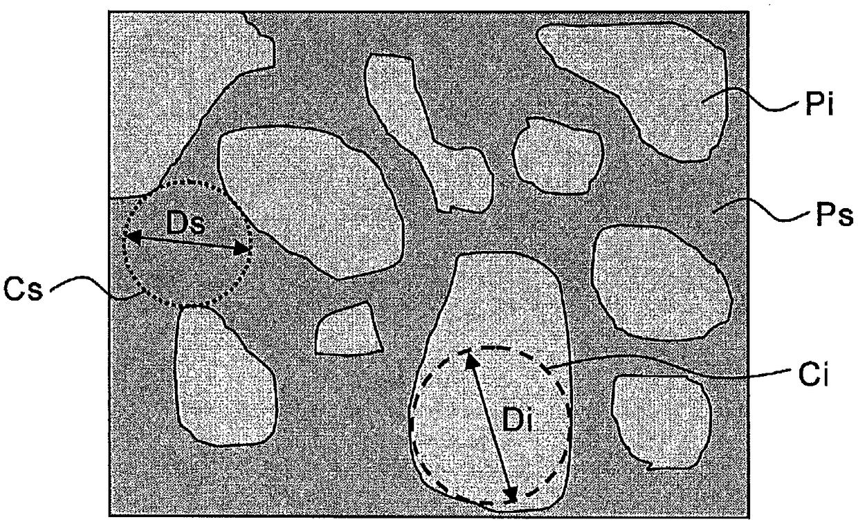
[0169] (SEM observation of phase separation structure and measurement of the maximum diam...
PUM
| Property | Measurement | Unit |
|---|---|---|
| thickness | aaaaa | aaaaa |
| width | aaaaa | aaaaa |
| length | aaaaa | aaaaa |
Abstract
Description
Claims
Application Information
 - R&D
- Intellectual Property
- Life Sciences
- Materials
- Tech Scout
- Unparalleled Data Quality
- Higher Quality Content
- 60% Fewer Hallucinations
Browse by: Latest US Patents, China's latest patents, Technical Efficacy Thesaurus, Application Domain, Technology Topic, Popular Technical Reports.
© 2025 PatSnap. All rights reserved.Legal|Privacy policy|Modern Slavery Act Transparency Statement|Sitemap|About US| Contact US: help@patsnap.com