Flexible display panel and preparation method thereof
A flexible display and flexible substrate technology, applied in nonlinear optics, optics, instruments, etc., can solve the problem of too wide trace width at the edge of the panel, and achieve the effect of reducing trace width, reducing non-display area, and reducing raw materials
- Summary
- Abstract
- Description
- Claims
- Application Information
AI Technical Summary
Problems solved by technology
Method used
Image

Examples
Embodiment 1
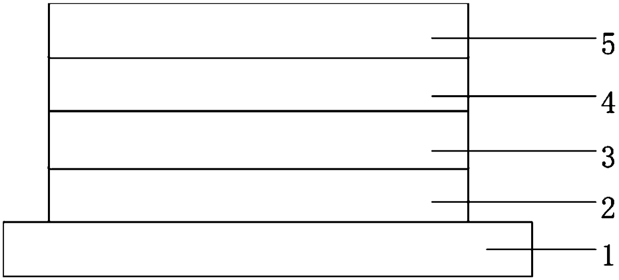
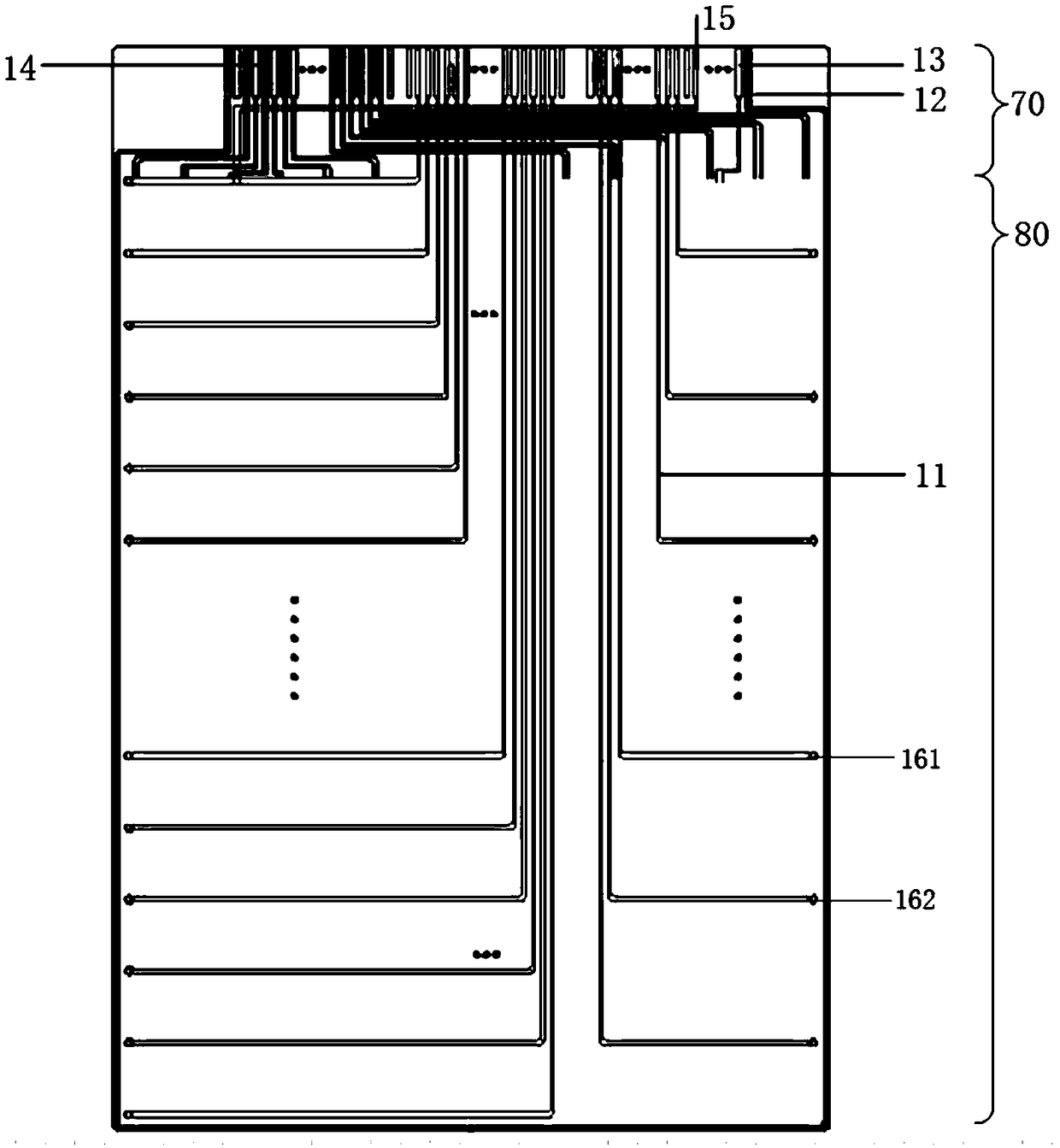
[0039] see figure 1 , figure 2 and image 3 , the present invention provides a flexible display panel, the surface of which defines a display area, a bonding area and a frame area, and the flexible display panel includes a flexible substrate 1 , a protective layer 2 , a semiconductor layer 3 , a light emitting layer 4 and a touch layer 5 .
[0040] The flexible substrate 1 in the display area is provided with gate leads 11, ground wires 12, touch sensing receiving electrode leads 13 and display area pads 80; the protective layer 2 in the frame area is provided with a first through hole 161 and a second through hole 162, the gate lead 11 is electrically connected to the gate in the semiconductor layer 3 through the first through hole 161, and the touch sensing receiving electrode lead 13 is electrically connected to the touch sensing receiving electrode in the touch layer 5 through the second through hole 162. sexual connection.
[0041] Wherein, the protective layer 2 is a...
Embodiment 2
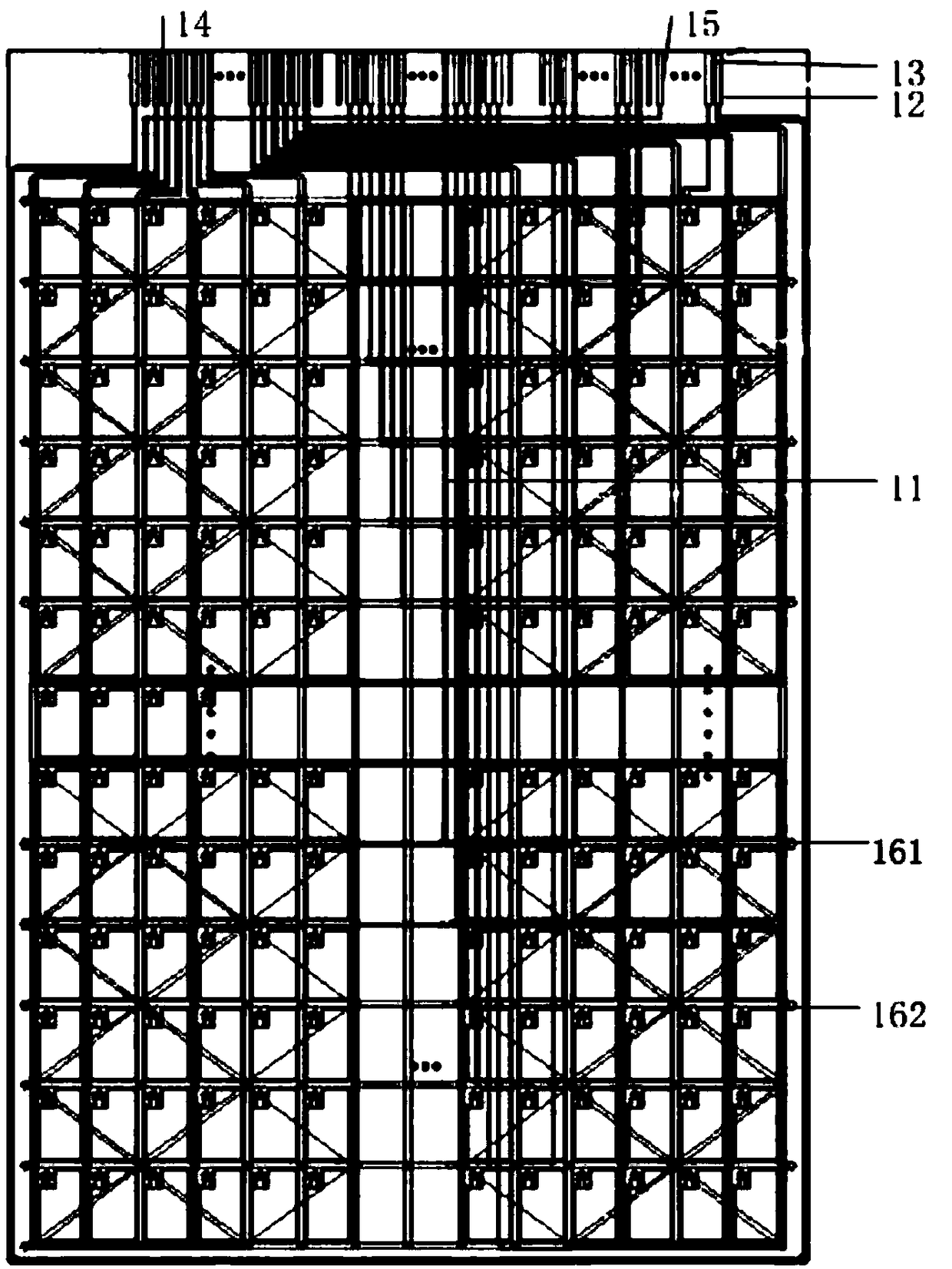
[0044] see figure 1 , Figure 4 and Figure 5 , the present invention provides another flexible display panel, the surface of which defines a display area, a bonding area and a frame area, and the flexible display panel includes a flexible substrate 1 , a protective layer 2 , a semiconductor layer 3 , a light emitting layer 4 and a touch layer 5 .
[0045] The flexible substrate 1 in the display area is provided with a gate lead 21, a ground wire 22, a touch sensing receiving electrode lead 23, a data lead 24, a touch sensing sending electrode lead 25, and a display area pad 80; the protective layer 2 in the frame area A first through hole 261, a second through hole 262, a third through hole 263, and a fourth through hole 264 are provided on the side of the first through hole 261, and the gate lead 21 is electrically connected to the gate in the semiconductor layer 3 through the first through hole 261. The touch sensing receiving electrode lead 23 is electrically connected t...
Embodiment 3
[0048] see Figure 6 , the present invention also provides a method for preparing a flexible display panel, comprising the following steps:
[0049] Step S11: Fabricate gate leads 11, ground wires 12, touch sensing receiving electrode leads 13 and display area pads 80 on the flexible substrate 1 in the display area;
[0050] Step S12: making a protective layer 2 on the flexible substrate 1, and making a first through hole 161 and a second through hole 162 at the edge of the protective layer 2 in the frame area;
[0051] Wherein, the protective layer 2 is an insulating layer, which protects all wirings on the flexible substrate 1;
[0052] Step S13: Fabricate the semiconductor layer 3 and the bonding area pad 70, and fabricate the data lead 14 at the same time, and electrically connect the gate lead 11 to the gate in the semiconductor layer 3 through the first through hole 161;
[0053] Wherein, the gate wire 11, the ground wire 12, and the touch sensing receiving electrode w...
PUM
 Abstract
Description
Claims
Application Information
 - R&D
- Intellectual Property
- Life Sciences
- Materials
- Tech Scout
- Unparalleled Data Quality
- Higher Quality Content
- 60% Fewer Hallucinations
Browse by: Latest US Patents, China's latest patents, Technical Efficacy Thesaurus, Application Domain, Technology Topic, Popular Technical Reports.
© 2025 PatSnap. All rights reserved.Legal|Privacy policy|Modern Slavery Act Transparency Statement|Sitemap|About US| Contact US: help@patsnap.com