Display panel and display device
A technology for display panels and display modules, which is used in identification devices, instruments, etc., and can solve problems such as unfavorable ultra-thinning
- Summary
- Abstract
- Description
- Claims
- Application Information
AI Technical Summary
Problems solved by technology
Method used
Image
Examples
Embodiment approach 1
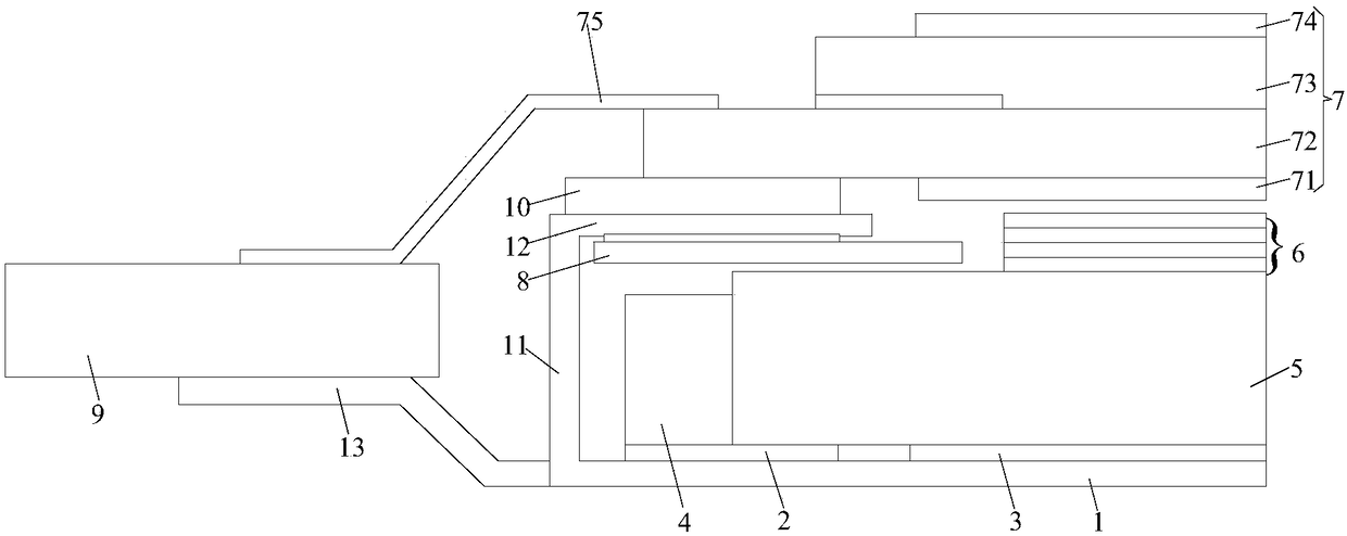
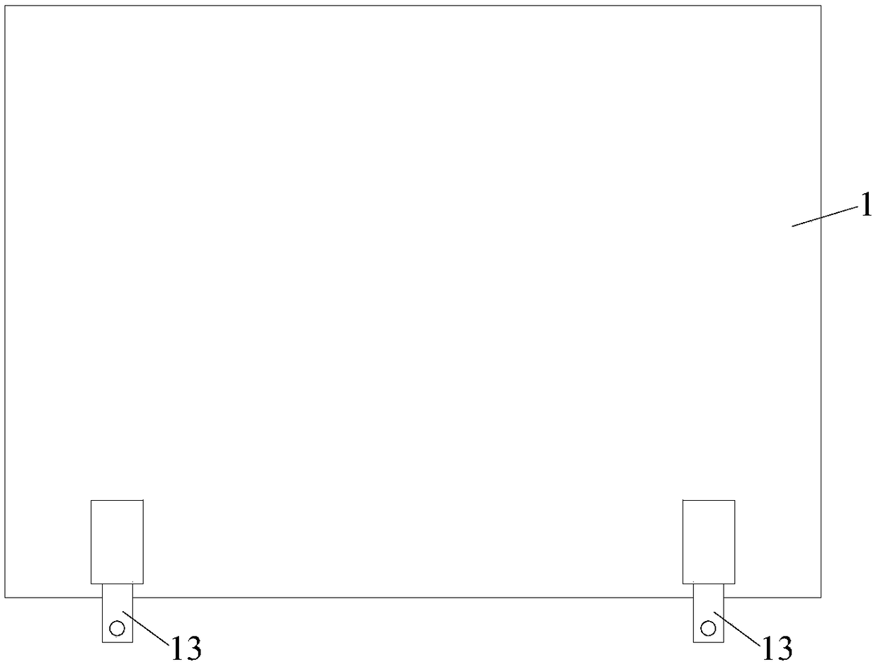
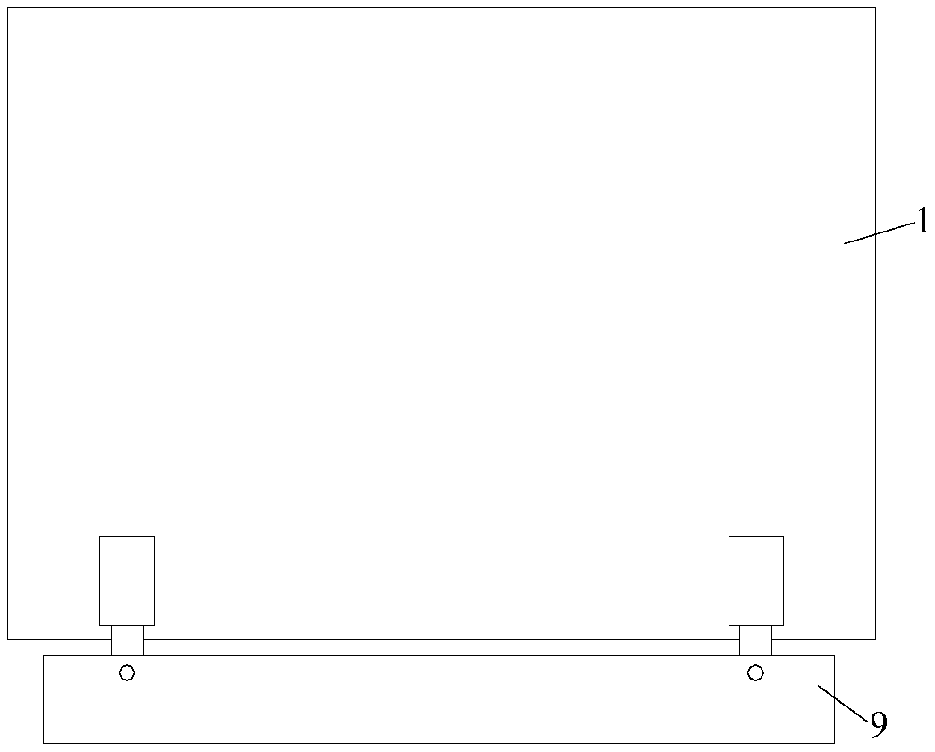
[0065] refer to Image 6 Shown is a schematic structural diagram of an embodiment of the display panel of the present invention; the display panel may include a backlight module and a display module 7 . refer to Figure 7 The schematic diagram of the structure of the backlight module shown, the backlight module can include a backplane 1, a circuit layer 2 and a white reflective sheet 3 are arranged on the backplane 1, and the circuit layer 2 forms a driving circuit for the light source 4; on the circuit layer 2 A light source 4 is provided on the side away from the backboard 1, and a light guide plate 5 is provided on the side of the white reflective sheet 3 away from the backboard 1, and the light guide plate 5 is located on the light emitting side of the light source 4; One side of the optical film layer 6 is provided, and the number of layers and the thickness of the optical film layer 6 can be set according to different layers and thicknesses. refer to Figure 8 The sch...
Embodiment approach 2
[0071] The structure of this exemplary embodiment is basically the same as that of the first exemplary embodiment, and the main difference lies in the structure of the backplane 1 . refer to Figure 11 As shown in the structural diagram of another embodiment of the display panel, since the circuit board 9 is relatively thin, the backplane 1 can be bent so that the circuit board 9 can support the display module 7 . The backplane 1 may include a backplane body 14 , a first bending structure 15 and a second bending structure 16 . The backplane body 14 is arranged in a flat shape, and is arranged under the white reflective sheet and the circuit layer 2 . The first bending structure 15 is connected to the backplane body 14 and extends toward a side close to the display module 7 . The second bending structure 16 is connected to the first bending structure 15 and extends in the same direction as the backplane body 14. The circuit board 9 is arranged on the second bending structure ...
Embodiment approach 3
[0073] The structure of this exemplary embodiment is basically the same as that of the first exemplary embodiment, and the main difference lies in the structure of the backplane 1 . refer to Figure 12 In the schematic structural diagram of another embodiment of the display panel shown, since the circuit board 9 is relatively thick, the backplane 1 can be bent so that the circuit board 9 can support the display module 7 . The backplane 1 may include a backplane body 14 , a first bending structure 15 and a second bending structure 16 . The backplane body 14 is arranged in a flat shape, and is arranged under the white reflective sheet and the circuit layer 2 . The first bending structure 15 is connected to the back panel body 14 and extends to a side away from the display module 7 . The second bending structure 16 is connected to the first bending structure 15 and extends in the same direction as the backplane body 14. The circuit board 9 is arranged on the second bending stru...
PUM
 Abstract
Description
Claims
Application Information
 - R&D Engineer
- R&D Manager
- IP Professional
- Industry Leading Data Capabilities
- Powerful AI technology
- Patent DNA Extraction
Browse by: Latest US Patents, China's latest patents, Technical Efficacy Thesaurus, Application Domain, Technology Topic, Popular Technical Reports.
© 2024 PatSnap. All rights reserved.Legal|Privacy policy|Modern Slavery Act Transparency Statement|Sitemap|About US| Contact US: help@patsnap.com


