Pixel circuit and display device

A technology of pixel circuit and charging unit, applied in static indicators, instruments, etc., can solve problems such as affecting the OLED current of the light-emitting element, uneven brightness of the OLED display, and decreased display quality.

Inactive Publication Date: 2019-02-19
KUNSHAN GO VISIONOX OPTO ELECTRONICS CO LTD
View PDF8 Cites 6 Cited by
  • Summary
  • Abstract
  • Description
  • Claims
  • Application Information

AI Technical Summary

Problems solved by technology

[0004] However, if figure 1 In the pixel circuit shown, when the charging phase of the transistor device M3 in the charging circuit ends and the light emitting phase starts, the channel charge of M3 is injected into the node P through the coupling, and the error ΔV1 is introduced to make the voltage V of point P P rise, which in turn affects the current of the light-emitting element OLED during the light-emitting phase
And because the M3 in each pixel circuit in the display screen is different, the error ΔV1 is also different, so this error will lead to uneven brightness in the OLED display screen and a decrease in display quality

Method used


Image

  • Pixel circuit and display device
  • Pixel circuit and display device
  • Pixel circuit and display device

Examples


Embodiment 1

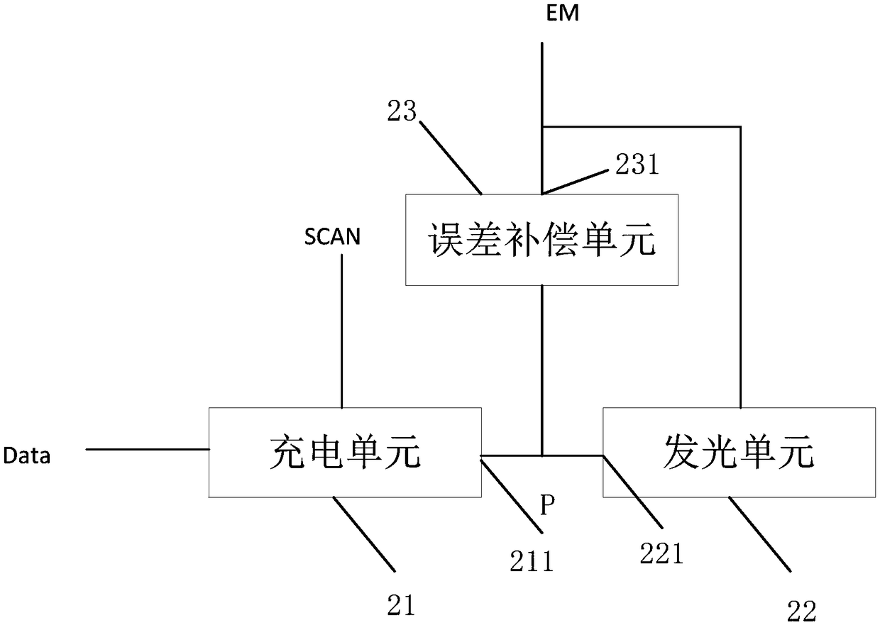
[0091] figure 2 It is a schematic structural diagram of a pixel circuit provided by Embodiment 1 of the present invention. Such as figure 2 As shown, the pixel circuit provided by the embodiment of the present invention includes: a charging unit 21, a light emitting unit 22 and an error compensation unit 23; wherein,

[0092] The voltage storage terminal 211 of the charging unit 21 is connected to the voltage input terminal 221 of the light emitting unit 22;

[0093] One end of the error compensation unit 23 is connected to the voltage storage terminal 211 of the charging unit 21, and the voltage of the voltage storage terminal 211 of the charging unit 21 is used to determine the magnitude of the current flowing through the light emitting unit 22;

[0094] The control terminal 231 of the error compensation unit 23 is used to receive the light-emitting control signal, and the light-emitting control signal is used to control the light-emitting unit 22 to emit light or stop e...

Embodiment 2

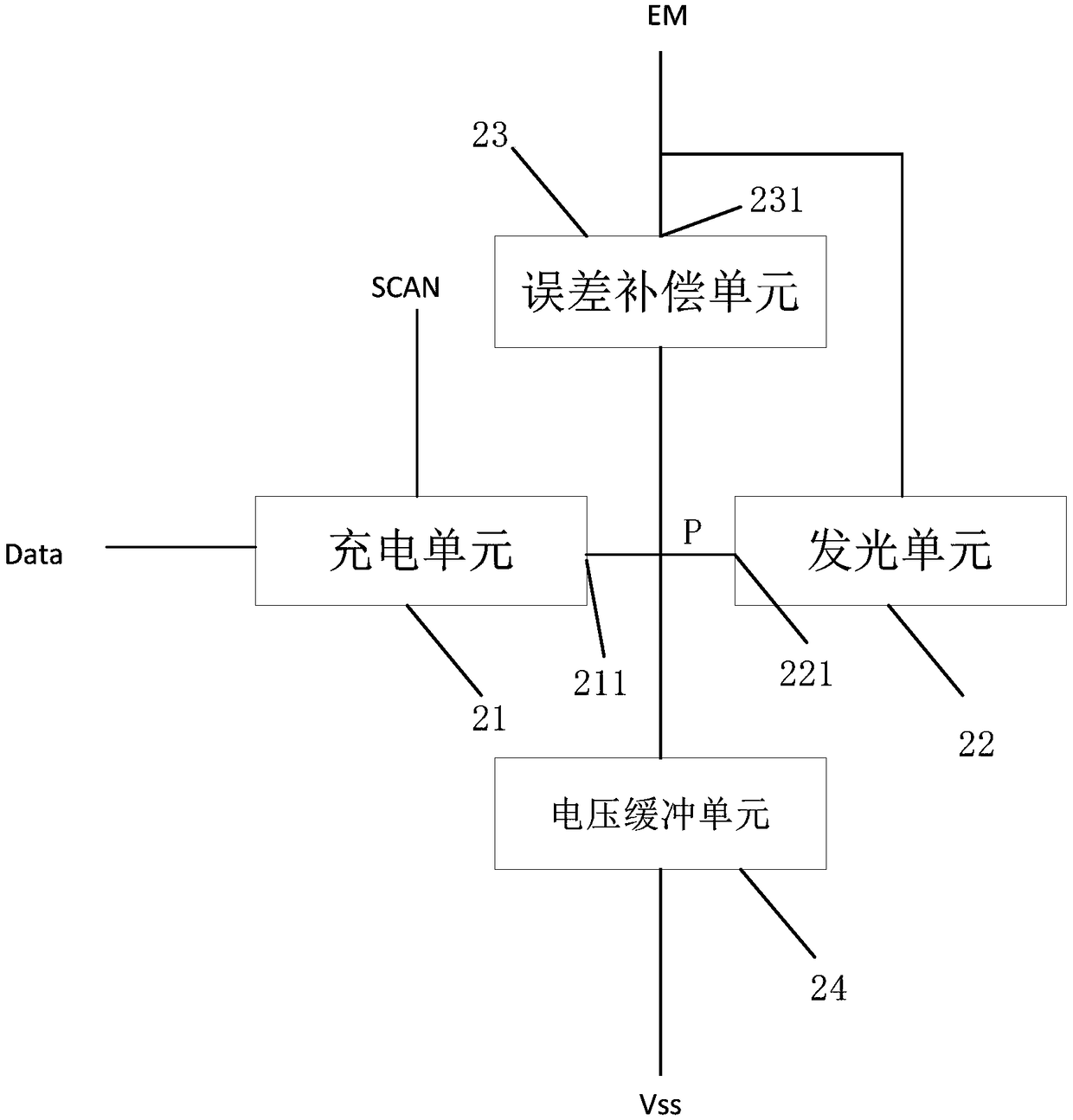
[0102] exist figure 1 On the basis of the illustrated embodiment, the embodiment of the present invention also provides a pixel circuit, image 3 It is a schematic structural diagram of the pixel circuit provided by Embodiment 2 of the present invention. Such as image 3 As shown, the pixel circuit further includes: a voltage buffer unit 24;

[0103] One end of the voltage buffer unit 24 is connected to the voltage storage terminal 211 of the charging unit 21, and the other end of the voltage buffer unit 24 is connected to the first DC power supply; the first DC power supply provides a negative voltage;

[0104] The voltage buffer unit 24 is used for slowing down the voltage variation of the voltage storage terminal 211 of the charging unit 21 when the charging unit 21 finishes charging and the light emitting control signal controls the light emitting unit 22 to emit light.

[0105] Exemplary, such as image 3 As shown, the pixel circuit provided by this embodiment, in fig...

Embodiment 3

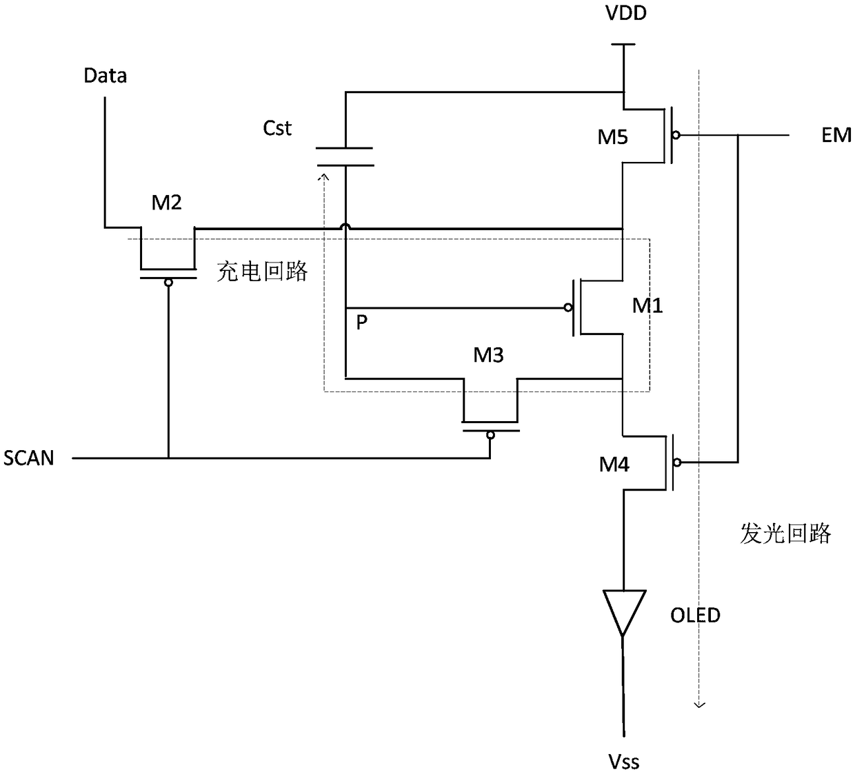
[0109] exist figure 2 or image 3 On the basis of the illustrated embodiments, the embodiment of the present invention further provides a pixel circuit. Figure 4 It is a schematic structural diagram of a pixel circuit provided by Embodiment 3 of the present invention. refer to Figure 4 As shown, the pixel circuit includes: a light emitting unit 22, a charging unit 21 and an error compensation unit 23; wherein,

[0110] The light emitting unit 22 includes: a first controllable element 31, a second controllable element 32, a third controllable element 33 and a light emitting element 34; the charging unit 21 includes: a fourth controllable element 35, a fifth controllable element 36 and a charging unit element 37;

[0111] The first end of the first controllable element 31 is connected to the second DC power supply VDD, the second end of the first controllable element 31 is connected to the first end of the second controllable element 32, and the first end of the second co...


PUM


Abstract

The invention provides a pixel circuit and a display device. The pixel circuit comprises a charging unit, a luminescence unit and an error compensation unit. The voltage storage end of the charging unit is connected to the voltage input end of the luminescence unit. One end of the error compensation unit is connected to the voltage storage end of the charging unit. The voltage of the voltage storage end of the charging unit is used for determining a current flowing through the luminescence unit. The control unit of the error compensation unit is used for receiving a luminescence control signal. The luminescence control signal is used for making the luminescence unit give out light or stop giving out light. The error compensation unit is used to reduce the voltage of the voltage storage endof the charging unit when the luminescence control signal makes the luminescence unit give out the light. Through adding the error compensation unit in the pixel circuit, the voltage rise of the voltage input end of the luminescence unit is reduced when a charging phase is ended and a luminescence phase is started so as to increase the brightness consistency of a display screen and improve display quality.

Description

technical field [0001] The present invention relates to the field of display technology, in particular to a pixel circuit and a display device. Background technique [0002] Organic Light Emitting Diode (OLED for short) display devices have the advantages of self-illumination, low driving voltage, thinness, fast response and high contrast, and are widely used in the display field. [0003] In the manufacturing process of OLED displays, due to technological reasons, there is usually a problem of uneven threshold voltage of transistor device parameters, which in turn leads to uneven brightness in the OLED display and a decrease in display quality. figure 1 It is a structural schematic diagram of an existing pixel circuit. Such as figure 1 The pixel circuit shown well solves the above problems. [0004] However, if figure 1 In the pixel circuit shown, when the charging phase of the transistor device M3 in the charging circuit ends and the light emitting phase starts, the ch...

Claims


Application Information

Patent Timeline
Patent Type & Authority Applications(China)
IPC IPC(8): G09G3/3233
CPCG09G3/3233G09G2320/0233G09G2300/0819G09G2300/0842G09G2300/0852G09G2300/0861G09G2320/045G09G3/3258G09G2300/0426
Inventor 赵国华金炳文胡思明韩珍珍朱晖
Owner KUNSHAN GO VISIONOX OPTO ELECTRONICS CO LTD
Why Eureka
Try Eureka