A silicon carbide insulated gate bipolar transistor

A bipolar transistor, insulated gate technology, applied in semiconductor devices, electrical components, circuits, etc., can solve the problems of large forward conduction resistance and low N-type cathode injection efficiency

Active Publication Date: 2021-06-08
UNIV OF ELECTRONICS SCI & TECH OF CHINA
View PDF4 Cites 0 Cited by
  • Summary
  • Abstract
  • Description
  • Claims
  • Application Information

AI Technical Summary

Problems solved by technology

[0004] The purpose of the present invention is to propose a silicon carbide insulated gate bipolar transistor for the problems of low N-type cathode injection efficiency and large forward conduction resistance of conventional silicon carbide insulated gate bipolar transistors

Method used


Image

  • A silicon carbide insulated gate bipolar transistor
  • A silicon carbide insulated gate bipolar transistor
  • A silicon carbide insulated gate bipolar transistor

Examples


Embodiment Construction

[0018] The present invention is described in detail below in conjunction with accompanying drawing

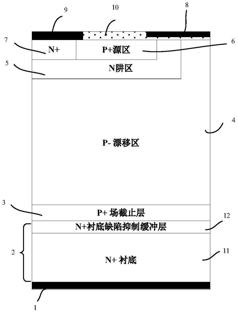
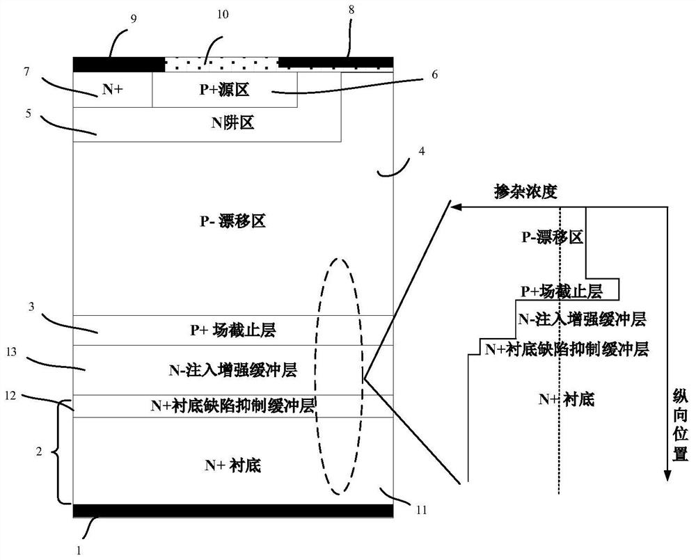
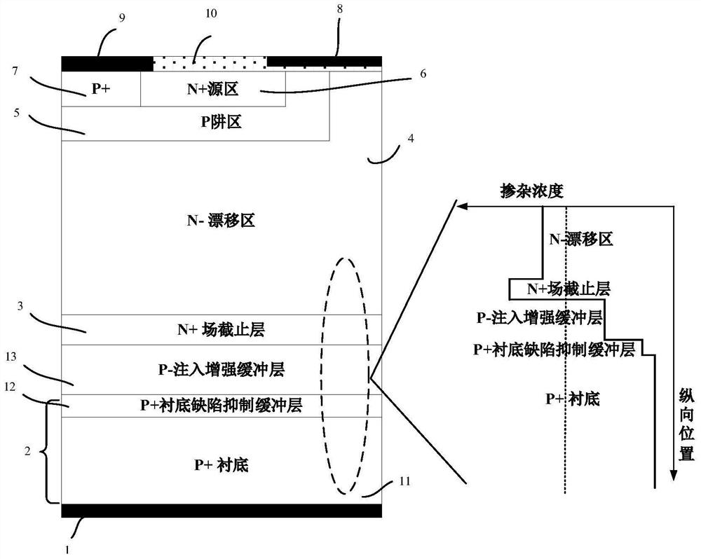
[0019] like figure 2 As shown, the silicon carbide insulated gate bipolar transistor of the present invention is a silicon carbide insulated gate bipolar transistor, and its cell structure includes an anode structure, a drift region structure, a gate structure and a cathode structure; for P-type silicon carbide Insulated gate bipolar transistor, its anode structure includes N+ ohmic contact region 7 and P+ source region 6 on its right side, and metal layer 9 on the upper surface of N+ ohmic contact region 7 and P+ source region; the gate The structure includes the N well region 5, the oxide layer 10 above the N well and the gate metal 8, the P+ source region 6 and the N+ ohmic contact region 7 in the anode structure are within the N well region 5; the drift region structure includes P - the drift region 4 and the P+ field stop layer 3 below it; the cathode structure is mainly...


PUM

PropertyMeasurementUnit
thicknessaaaaaaaaaa

Abstract

The invention relates to power semiconductor technology, in particular to a silicon carbide insulating gate bipolar transistor. The present invention transforms the cathode region of a conventional silicon carbide IGBT by adding an N-IEB layer (N type-Injection Enhanced Buffer layer, N-type injection enhanced buffer layer) under the P+ field stop layer. The layer doping concentration is low, which improves the minority carrier lifetime and mobility in this region, thereby increasing the minority carrier diffusion length in the cathode structure, thereby increasing the cathode injection efficiency. And because the built-in electric field will be generated due to the concentration difference between the N-type substrate and the N-type injection-enhanced buffer layer, its direction is directed from the N-type substrate to the N-type injection-enhanced buffer layer, preventing the minority carrier holes from being injected by the N-type enhanced buffer layer. layer diffuses to the N-type substrate, thereby reducing the minority carrier hole diffusion current, and thus increasing the cathode injection efficiency.

Description

technical field [0001] The invention belongs to the technical field of power semiconductors, in particular to a silicon carbide insulated gate bipolar transistor Background technique [0002] As a relatively mature power electronic device, the insulated gate bipolar transistor has been widely used in high-power applications such as AC motors, frequency converters, switching power supplies, lighting circuits, traction drives and other fields. Insulated gate bipolar transistor is also an important device used in pulsed power technology. [0003] Insulated gate bipolar transistor, referred to as IGBT, is a hybrid power electronic device consisting of a power MOS field effect transistor and a bipolar transistor. It has the characteristics of combining MOS and bipolar with MOS input and bipolar output functions. The MOSFET structure is used to provide base drive current to the bipolar junction transistor. At the same time, the bipolar junction transistor modulates the conductivi...

Claims


Application Information

Patent Timeline
Patent Type & Authority Patents(China)
IPC IPC(8): H01L29/739
CPCH01L29/7395
Inventor 陈万军谯彬高吴昊张柯楠夏云刘超
Owner UNIV OF ELECTRONICS SCI & TECH OF CHINA
Why Eureka
Try Eureka