
Liquid crystal display panel and preparation method thereof

A liquid crystal display panel, color film substrate technology, applied in the direction of nonlinear optics, instruments, optics, etc., can solve the problems of affecting camera quality, limitation, high cost, etc., to increase light export and light output efficiency, increase light export, reduce The effect of total reflection

Inactive Publication Date: 2019-02-15
WUHAN CHINA STAR OPTOELECTRONICS TECH CO LTD
View PDF4 Cites 4 Cited by
  • Summary
  • Abstract
  • Description
  • Claims
  • Application Information

AI Technical Summary

Problems solved by technology

However, the current development of in-plane hole-digging technology is limited by the current cutting and drilling technology. Therefore, there are still no response products on the market.
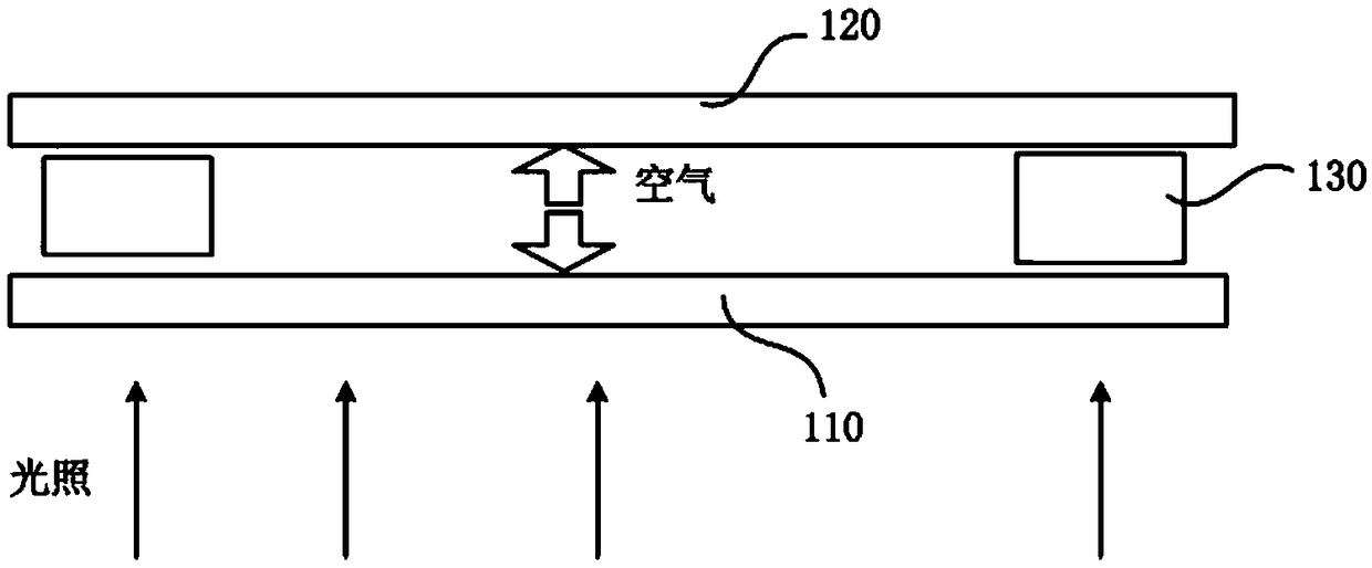
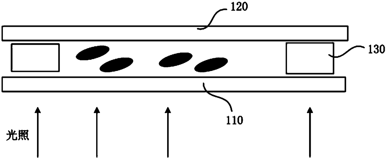
[0003] There are two known in-plane digging schemes: one is the blind hole scheme, such as Figure 1A , 1B As shown, the camera is installed under the blind hole, but this solution is limited by the penetration rate of glass, liquid crystal and film, and will affect the camera quality and reduce customer experience
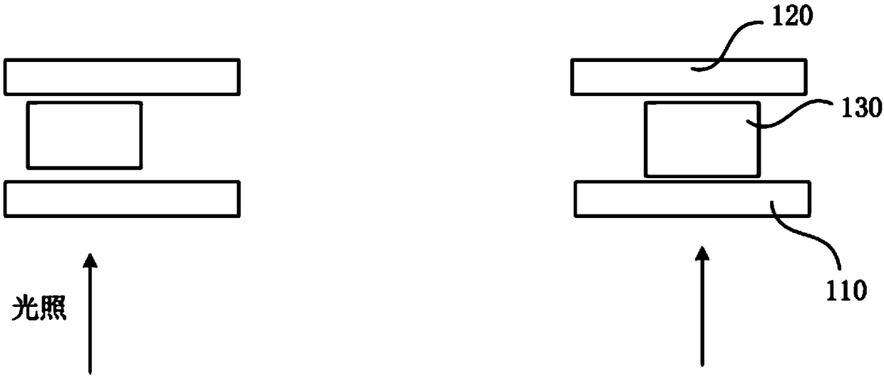
The other is the digging scheme, such as figure 2 As shown, but this solution is limited by the mass production laser grinding process, the life of the grinding rod is limited, and it will be affected by debris and heat radiation areas. In addition, the cost of this solution is relatively high

Method used


Image

  • Liquid crystal display panel and preparation method thereof
  • Liquid crystal display panel and preparation method thereof
  • Liquid crystal display panel and preparation method thereof

Examples


Embodiment Construction

[0024] The following will clearly and completely describe the technical solutions in the embodiments of the present invention with reference to the drawings in the embodiments of the present invention. Apparently, the described embodiments are only some of the embodiments of the present invention, but not all of them. Based on the embodiments of the present invention, all other embodiments obtained by those skilled in the art without creative efforts fall within the protection scope of the present invention.

[0025] The terms "first", "second", "third", etc. (if any) in the description and claims of the present invention and the above drawings are used to distinguish similar objects and not necessarily to describe a specific order or sequentially. It should be understood that the items so described are interchangeable under appropriate circumstances. Furthermore, the terms "comprising" and "having", as well as any variations thereof, are intended to cover a non-exclusive in...


PUM


Abstract

The invention discloses a liquid crystal display panel and a preparation method thereof. The liquid crystal display panel comprises: a color film substrate which is a light transmissive substrate, andan array substrate. The array substrate and the color film substrate are arranged relative to each other and are spaced apart. A sealing layer is arranged between the color film substrate and the array substrate, and has a hollow structure to form a mounting hole. The sealing layer is for isolating the mounting hole from a liquid crystal arranged between the color film substrate and the array substrate. A position on the array substrate corresponding to the mounting hole is open, and a position of the inner surface of the color film substrate corresponding to the mounting hole is arcuate.

Description

technical field [0001] The invention relates to the technical field of liquid crystal display, in particular to a liquid crystal display panel and a preparation method thereof. Background technique [0002] The LCD industry has developed rapidly in recent years, and various new special designs and special-shaped mobile phone displays have gradually occupied a larger share in the market. Various mobile phone manufacturers have launched more and more new designs, such as notch screen, beauty tip, water drop screen, drilling screen (that is, digging holes in the plane), and many other new designs emerge in endlessly. However, the development of in-plane hole-digging technology is currently limited by the current cutting and drilling technology. Therefore, there are still no responsive products on the market. [0003] There are two known in-plane digging schemes: one is the blind hole scheme, such as Figure 1A , 1B As shown, the camera is installed under the blind hole, but t...

Claims


Application Information

Patent Timeline
Patent Type & Authority Applications(China)
IPC IPC(8): G02F1/1333G02F1/1335G02F1/1339
CPCG02F1/1333G02F1/133553G02F1/1339G02F1/13394
Inventor 程薇
Owner WUHAN CHINA STAR OPTOELECTRONICS TECH CO LTD
Learn More