A liquid crystal display panel and its manufacturing method

A technology for liquid crystal display panels and substrates, which is applied in instruments, nonlinear optics, optics, etc., and can solve the problems of lowering the accuracy of the identification pair, the operation and identification affecting the rapid abnormal response of the product, and the inability to read the pair accuracy. Conducive to diversity, improve visual management, and improve product quality

Active Publication Date: 2021-12-03
TCL CHINA STAR OPTOELECTRONICS TECH CO LTD
View PDF7 Cites 0 Cited by
  • Summary
  • Abstract
  • Description
  • Claims
  • Application Information

AI Technical Summary

Problems solved by technology

[0005] The alignment accuracy of the existing technology needs to be identified on a high-power microscope and then specifically identify which alignment mark on the TFT substrate and the CF substrate is the most accurate in order to read the alignment accuracy. Errors in operation and identification have seriously affected the rapid abnormal response of the product
Especially when the size of the panel is too large and the microscope is too small to cope with the situation, the matching accuracy cannot be easily read out on the machine, and the efficiency of identifying the matching accuracy is reduced

Method used


Image

  • A liquid crystal display panel and its manufacturing method
  • A liquid crystal display panel and its manufacturing method
  • A liquid crystal display panel and its manufacturing method

Examples


Embodiment Construction

[0034] The following descriptions of the various embodiments refer to the accompanying drawings to illustrate specific embodiments in which the invention may be practiced. The directional terms mentioned in the present invention, such as [top], [bottom], [front], [back], [left], [right], [inside], [outside], [side], [horizontal], etc. , are for orientation only with reference to the attached drawings. Therefore, the directional terms used are used to illustrate and understand the present invention, but not to limit the present invention. In the drawings, units with the same name or similar structures are denoted by the same reference numerals.

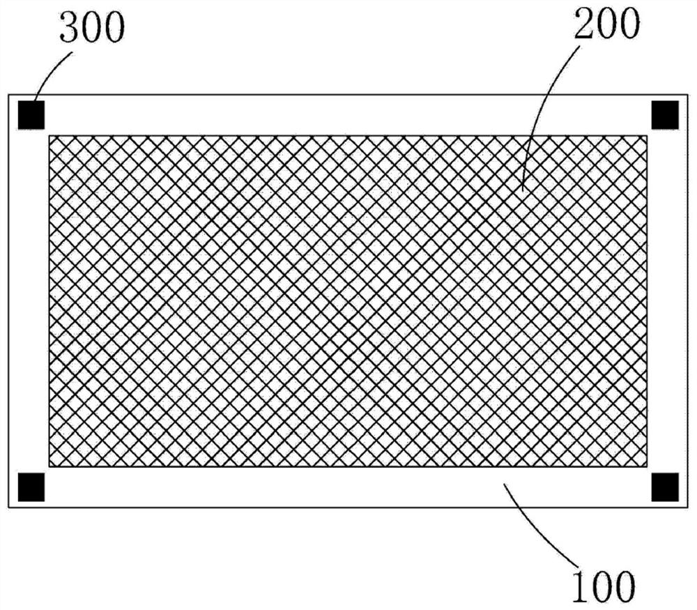
[0035] One embodiment of the present invention provides a liquid crystal display panel, which includes a TFT substrate and a CF substrate, wherein a first group-to-group mark is provided on the TFT substrate, and a second group-to-group mark is correspondingly provided on the CF substrate.

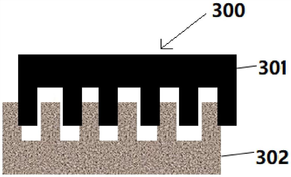
[0036] see image 3 As shown, wherein the...


PUM


Abstract

The invention provides a liquid crystal display panel, including a TFT substrate and a CF substrate, wherein a first group-to-group mark is arranged on the TFT substrate, and the first group-to-group mark includes an upper first mark and an upper second mark; A second group of group-to-group marks is set, which includes the first lower mark, the second lower mark, the first mark down, and the second mark down, wherein the first mark down is correspondingly set under the first mark down, and the side of the first mark The side is flush with the side of the lower first logo, the lower second mark is correspondingly arranged under the lower second logo, and the side of the lower second mark is flush with the side of the lower second logo. The advantage of the present invention is that by arranging a new pairing mark on the TFT board and the CF board, the grouping method between the grouping marks set on the TFT board and the CF board is further improved, so that it can be easily placed on the machine or anywhere To read out the alignment accuracy, it is not necessary to move the aligned display panel under a high-power microscope to read the alignment accuracy.

Description

technical field [0001] The invention relates to the field of liquid crystal display technology, in particular to a liquid crystal display panel therein. Background technique [0002] The thin film transistor liquid crystal display panel is composed of a thin film transistor (TFT, Thin Film Transistor) and a color filter (CF, Color Filter), wherein the TFT substrate and the CF substrate are set up and down oppositely, wherein the TFT substrate and the CF substrate The alignment accuracy of the substrate is related to the quality of the product. If the vertical misalignment between the TFT substrate and the CF substrate is too large, it will affect the light leakage of the panel pixels and cause the screen to become white, which will affect the product yield. [0003] Such as figure 1 As shown, in the traditional liquid crystal display panel structure, the first process of the CF substrate 100 is to form a black matrix (Black Matrix, BM) 200, and the black matrix 200 will for...

Claims


Application Information

Patent Timeline
Patent Type & Authority Patents(China)
IPC IPC(8): G02F1/1333G02F1/13
CPCG02F1/1303G02F1/1333G02F1/133354
Inventor 罗忠云
Owner TCL CHINA STAR OPTOELECTRONICS TECH CO LTD
Why Eureka
Try Eureka