A Method for Measurement of Semiconductor Material Properties Based on Free Carrier Absorption Imaging

A technology of carrier absorption and material properties, applied in the direction of measurement devices, analysis materials, material excitation analysis, etc., can solve the problems of insufficient measurement technology of semiconductor material properties, and achieve the effects of avoiding errors, simple measurement devices, and high measurement accuracy

Active Publication Date: 2020-11-17
XIAN TECH UNIV
View PDF11 Cites 0 Cited by
  • Summary
  • Abstract
  • Description
  • Claims
  • Application Information

AI Technical Summary

Problems solved by technology

[0004] The present invention provides a semiconductor material characteristic measurement method based on free carrier absorption imaging in order to solve the deficiencies of the existing semiconductor material characteristic measurement technology

Method used


Image

  • A Method for Measurement of Semiconductor Material Properties Based on Free Carrier Absorption Imaging
  • A Method for Measurement of Semiconductor Material Properties Based on Free Carrier Absorption Imaging
  • A Method for Measurement of Semiconductor Material Properties Based on Free Carrier Absorption Imaging

Examples


Embodiment Construction

[0020] In order to make the object, technical solution and advantages of the present invention clearer, the present invention will be further described in detail below in conjunction with the accompanying drawings and embodiments. It should be understood that the specific embodiments described here are only used to explain the present invention, not to limit the present invention.

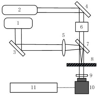
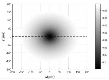
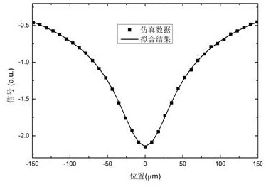
[0021] Principle of the present invention is:

[0022] The Gaussian-distributed continuous pump laser with photon energy greater than the semiconductor bandgap width is focused and irradiated on the surface of the semiconductor material, which is absorbed by the semiconductor material to generate excess free carriers. When another beam of photon energy is lower than the semiconductor bandgap width When the continuous probing laser is incident on the same position of the material, the intensity of the probing beam decreases after passing through the semiconductor material due to the absorption of th...


PUM

PropertyMeasurementUnit
wavelengthaaaaaaaaaa
reflectanceaaaaaaaaaa

Abstract

The invention relates to a measurement method for semiconductor material characteristics based on free carrier absorption imaging and solves the problems of defect of an existing semiconductor material characteristic measurement technology. The method adopted by the invention comprises the steps of (1) vertically irradiating continuous detection laser light to a surface of a measured semiconductorsample, measuring by a near-infrared camera and recording the transmitted detection light intensity spatial distribution S0 at this time by a computer; (2) vertically irradiating the focused continuous pumping laser light to a center position of a sample detection light radiation region, measuring by the near-infrared camera and recording the transmitted detection light intensity spatial distribution S1 at this time by the computer, wherein the size of a detection laser light beam incident to the surface of the sample is greater than the size of a pumping laser light beam focusing on the surface of the sample; (3) processing the transmitted detection light intensity spatial distribution imaging results S0 and S1 obtained in steps (1) and (2), that is S=(S1-S0) / S0; and (4) intercepting measurement data having different distances to a peak value along the peak position of the free carrier absorption imaging result to obtain multiple characteristic parameters of the to-be-measured sample.

Description

technical field [0001] The invention relates to the technical field of semiconductor material characteristic measurement, in particular to a semiconductor material characteristic measurement method based on free carrier absorption imaging. Background technique [0002] The development of semiconductor raw materials in the direction of large diameter and low defect, and the continuous improvement of the integration level of microelectronic devices have prompted higher and higher requirements for material processing technology and performance testing. In order to ensure that materials can be used in devices and improve device stability and yield, accurate and rapid on-line monitoring and non-destructive characterization of material properties are required in the material processing process. Photo-Carrier Radiation (PCR: Photo-Carrier Radiometry) technology and Modulated Free-Carrier Absorption (MFCA: Modulated Free-Carrier Absorption) technology are two optical non-destructive...

Claims


Application Information

Patent Timeline
Patent Type & Authority Patents(China)
IPC IPC(8): G01N21/63
CPCG01N21/636G01N2201/06113G01N2201/102
Inventor 王谦刘卫国
Owner XIAN TECH UNIV
Why Eureka
Try Eureka