Storage and transfer device for chips

A transfer device and chip technology, applied in the direction of transportation and packaging, conveyor objects, etc., can solve the problems of automatic wafer transfer, inconvenient operation, etc., and achieve the effect of cost saving, simple and convenient structure

Active Publication Date: 2020-08-21
泸州龙芯微科技有限公司
View PDF4 Cites 0 Cited by
  • Summary
  • Abstract
  • Description
  • Claims
  • Application Information

AI Technical Summary

Problems solved by technology

During processing, such as polishing the wafer, the wafers in the box need to be manually taken to the processing table one by one for processing, which is inconvenient to operate
However, there is no device that can automatically transfer the wafers in the box to the processing table.

Method used


Image

  • Storage and transfer device for chips
  • Storage and transfer device for chips
  • Storage and transfer device for chips

Examples


Embodiment Construction

[0016] The following is further described in detail through specific implementation methods:

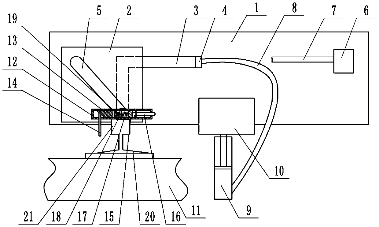
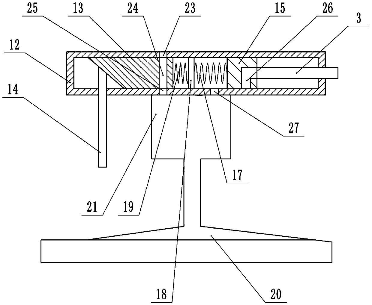
[0017] The reference signs in the drawings of the description include: vertical board 1, sliding board 2, bending hole 3, extrusion air bag 4, inclined hole 5, suction pump 6, pipe body 7, air pipe 8, cavity body 9, box body 10 , processing table 11, horizontal plate 12, wedge 13, vertical rod 14, moving block 15, suction pipe 16, second compression spring 17, partition 18, first compression spring 19, suction cup 20, connecting block 21, horizontal Rod 22 , second pressurized air hole 23 , pressurized air channel 24 , first pressurized air hole 25 , air intake channel 26 , air intake hole 27 .

[0018] The embodiment is basically as attached Figure 1-Figure 3 As shown: the storage and transfer device for chips, including a frame, a vertical plate 1 is welded on the frame, and a bending hole 3 is arranged on the vertical plate 1. The bending hole 3 in this embodiment includes a hor...


PUM


Abstract

The invention relates to the field of machining of chips, in particular to a chip storage and transfer device. The chip storage and transfer device comprises a vertical plate, a bent hole is formed inthe vertical plate, a sliding plate is slidingly connected to the vertical plate, an oblique hole is formed in the sliding plate, a cross bar penetrates through the oblique hole and the bent hole andis provided with a sucker mechanism, and a machining table is arranged below the vertical plate; a piston mechanism is arranged below one end of the bent hole and comprises a cavity, a piston slidingly connected in the cavity and a piston rod connected to the piston; a box body with an opening in the top is placed at the end, away from the piston, of the piston rod; an extrusion airbag is arranged at the end, above the box body, of the bent hole; an air pipe is communicated between the extrusion airbag and the cavity, a first one-way air inlet valve is arranged on the extrusion airbag, a second one-way air inlet valve is connected between the air pipe and the cavity, and a control valve is arranged on the cavity. According to the scheme, automatic transfer of wafers in the box body is achieved.

Description

technical field [0001] The invention relates to the field of chip processing, in particular to a storage and transfer device for chips. Background technique [0002] Wafer refers to the silicon wafer used in the production of silicon semiconductor integrated circuits. Because of its circular shape, it is called a wafer. Currently, wafers are stored in boxes. During processing, such as polishing the wafer, the wafers in the box need to be manually taken to the processing table one by one for processing, which is inconvenient to operate. However, there is no device that can automatically transfer the wafers in the box to the processing table. Contents of the invention [0003] The object of the present invention is to provide a storage and transfer device for chips to realize automatic transfer of wafers in a box. [0004] In order to achieve the above object, the technical solution of the present invention is: a storage and transfer device for chips, including a vertical...

Claims


Application Information

Patent Timeline
Patent Type & Authority Patents(China)
IPC IPC(8): B65G47/91
CPCB65G47/912
Inventor 黄晓波
Owner 泸州龙芯微科技有限公司
Why Eureka
Try Eureka