Phase-change heat dissipation chip structure and manufacturing method thereof
A chip structure and phase change technology, applied in electrical components, electric solid devices, circuits, etc., can solve problems such as chip stress, achieve the effects of reducing area, reducing pressure, and improving heat dissipation efficiency
- Summary
- Abstract
- Description
- Claims
- Application Information
AI Technical Summary
Problems solved by technology
Method used
Image

Examples
Embodiment approach
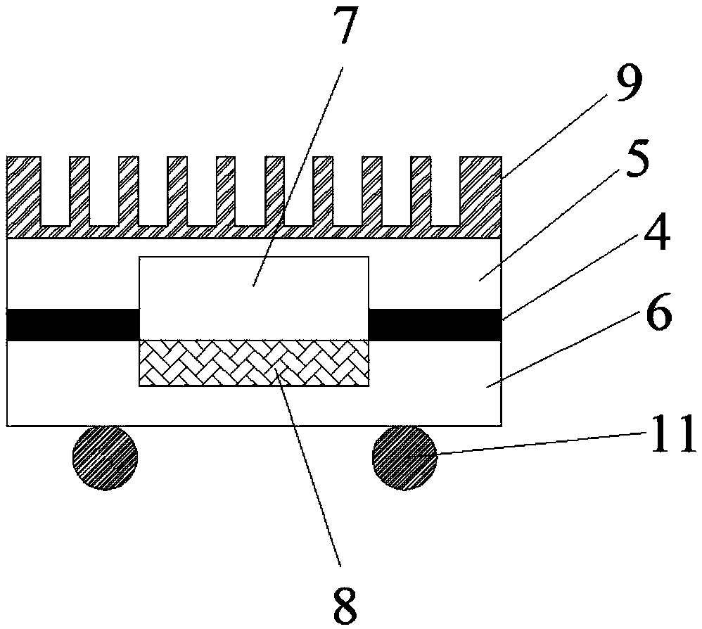
[0061] According to one embodiment of the present invention, a phase change heat dissipation chip structure is provided, including a cover plate and a wafer:
[0062] refer to figure 1 , the lower surface of the cover plate 5 is bonded to the back surface of the wafer 6, the lower surface of the cover plate 5 is provided with a cavity 7, the back surface of the wafer 6 is provided with a cavity 8, the cavity 7 communicates with the cavity 8, and the cavity 7 or There is a phase change material stored in the empty slot 8 .
[0063] At this stage, the main improvement direction for phase change heat dissipation is to improve the heat transfer capacity of phase change materials. According to the phase change temperature point, select the appropriate phase change material. After the phase change material absorbs heat, it will undergo a solid-to-liquid transition or a liquid-to-gas transition. , so as to maintain the slow temperature rise of the chip.
[0064] The solid phase cha...
Embodiment 1
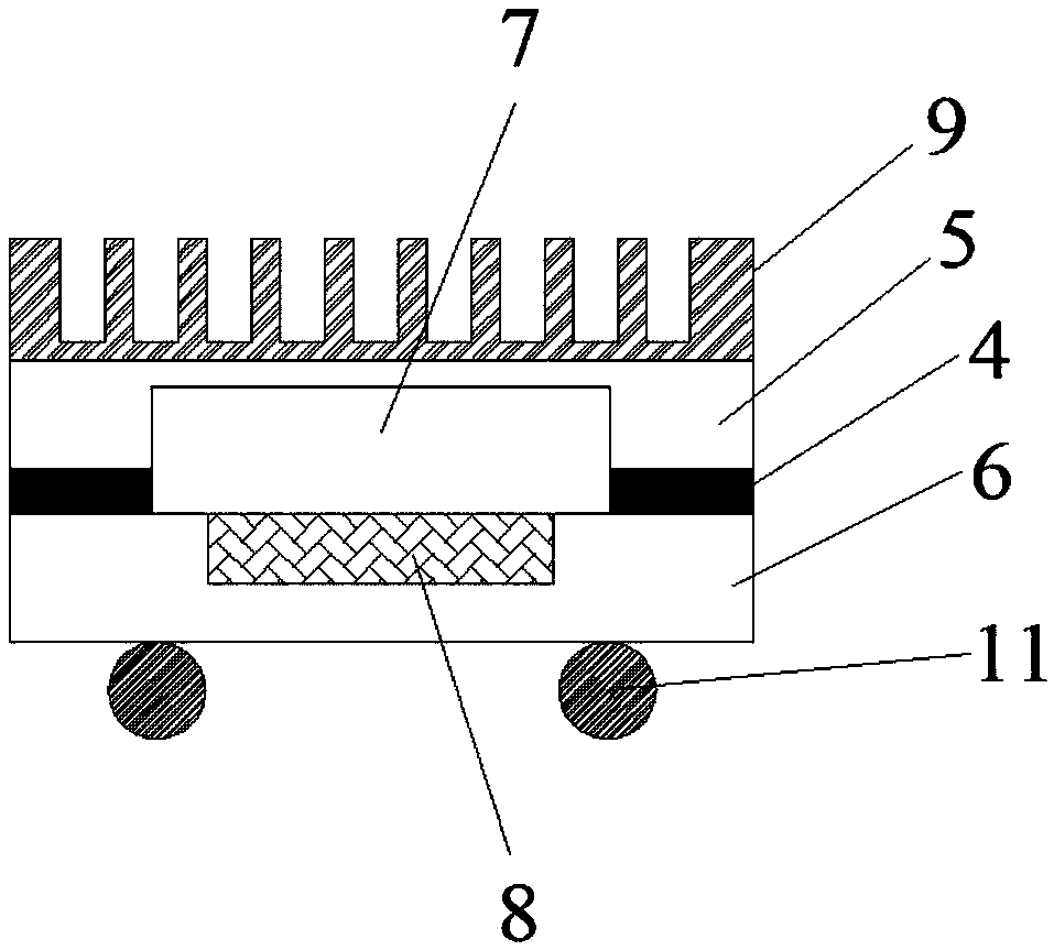
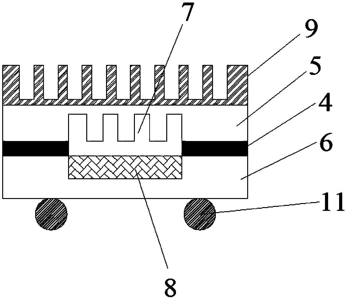
[0152] figure 1 According to an embodiment of the present invention, the structure of the phase-change heat dissipation chip, figure 2 A phase-change heat dissipation chip structure according to an embodiment of the present invention, image 3 Another phase change heat dissipation chip structure according to an embodiment of the present invention.
[0153] like figure 1 As shown, the embodiment provides a phase change heat dissipation chip structure, including a cover plate 5 and a wafer 6:
[0154] The lower surface of the cover plate 5 is bonded to the back surface of the wafer 6, the lower surface of the cover plate 5 is provided with a cavity 7, the back surface of the wafer 6 is provided with a cavity 8, the cavity 7 communicates with the cavity 8, and the cavity 7 or the cavity The slot 8 contains a phase change material.
[0155] The structure also includes a heat sink 9 disposed on the upper surface of the cover plate 5 ; and a conductive bump 11 mounted on the fr...
Embodiment 2
[0160] Figure 4 A flowchart of a wafer-level manufacturing method for phase change heat dissipation according to an embodiment of the present invention. Figure 5(A) ~ Figure 5(F) They are schematic structural diagrams of different stages in the wafer-level manufacturing process of phase change heat dissipation according to an embodiment of the present invention.
[0161] like Figure 4 As shown, this embodiment provides a wafer-level preparation method for phase change heat dissipation, including the following steps:
[0162] Step 101: Provide a wafer 201, etch the back of the wafer 101 to form a plurality of hollow grooves 103, and the depth of the hollow grooves 203 does not touch the deep well region close to the wafer 201, as shown in FIG. 5(A) ;
[0163] Etching the back of the wafer 201 to form a plurality of empty grooves 203, the back of the wafer 201 needs to be thinned;
[0164] Step 102: Provide a cover plate 202 with the same size as the wafer 201, etch the l...
PUM
 Abstract
Description
Claims
Application Information
 - R&D
- Intellectual Property
- Life Sciences
- Materials
- Tech Scout
- Unparalleled Data Quality
- Higher Quality Content
- 60% Fewer Hallucinations
Browse by: Latest US Patents, China's latest patents, Technical Efficacy Thesaurus, Application Domain, Technology Topic, Popular Technical Reports.
© 2025 PatSnap. All rights reserved.Legal|Privacy policy|Modern Slavery Act Transparency Statement|Sitemap|About US| Contact US: help@patsnap.com