An LGA device printing patch auxiliary device
An auxiliary device and patch technology, which is applied in the direction of assembling printed circuits, printed circuits, and printed circuits with electrical components, can solve the problems of difficulty in making chip-level stencil tooling, low success rate of solder paste printing, and high difficulty in manufacturing processes. Achieve the effects of reducing the risk of tin bead hidden dangers, reducing the difficulty and cost of production, and making the production process less difficult
- Summary
- Abstract
- Description
- Claims
- Application Information
AI Technical Summary
Problems solved by technology
Method used
Image

Examples
Embodiment 1
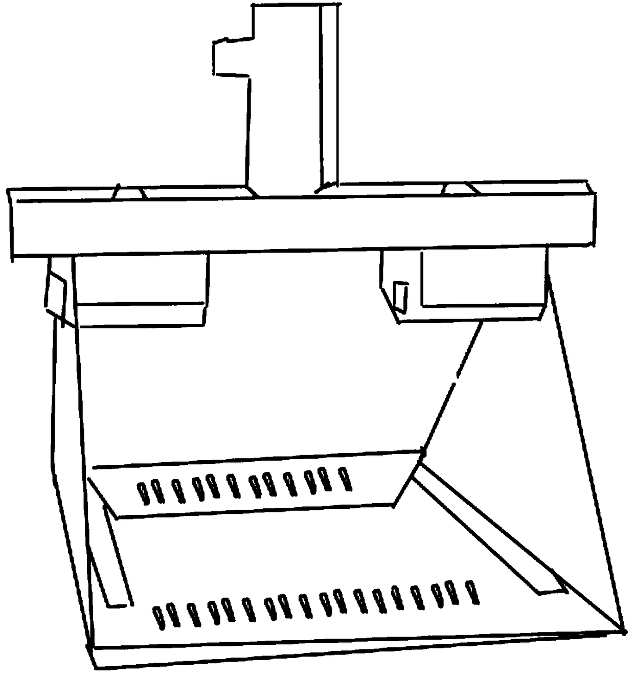
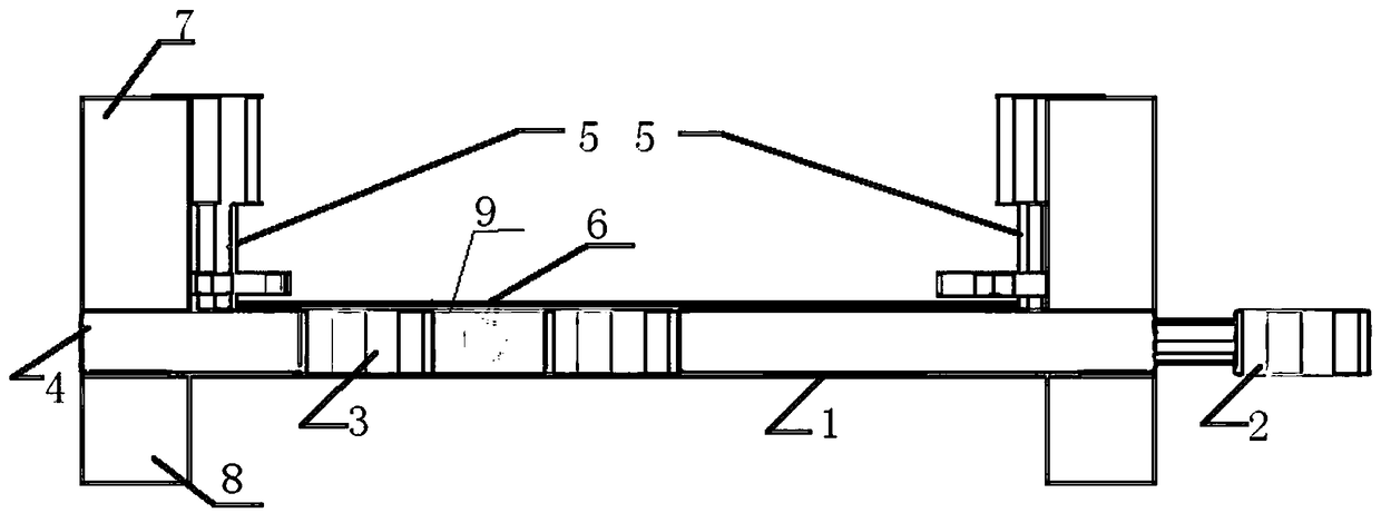
[0030] An auxiliary device for LGA device printing and patching includes a chip 10, a squeegee blade, and a chip-level steel mesh 6. The LGA device printing and patching auxiliary device at least further includes an auxiliary steel sheet 1, a chip X-axis direction connector 2, and a chip Y Axis direction connector 3, base 4, Z-axis direction adjustment connector 5, multiple upper support seats 7 and multiple lower support seats 8, upper support seats 7 are connected to the corners of the base 4, the base 4 The bottom corners are all connected with a lower support base 8, a hole 9 is opened in the middle of the base 4, the chip 10 is horizontally connected to the hole 9 through the chip X-axis direction connector 2, and the chip 10 is longitudinally passed through the chip Y-axis direction connector 3 is connected to the hole 9, the left and right ends of the upper middle of the base 4 are connected to the Z-axis direction adjustment connector 5, the chip-level steel mesh 6 is co...
Embodiment 2
[0032] Such as Figure 3-7 As shown, an auxiliary device for printing and attaching an LGA device includes a chip 10, a squeegee blade, and a chip-level steel mesh 6. The auxiliary device for printing and attaching an LGA device at least further includes an auxiliary steel sheet 1 and a chip X-axis direction connector 2 , Chip Y-axis direction connector 3, base 4, Z-axis direction adjustment connector 5, multiple upper support seats 7 and multiple lower support seats 8, upper support seats 7 are connected to the corners of the base 4 , The lower support base 8 is connected to the corners below the base 4, the middle of the base 4 is provided with a hole 9, the chip 10 is connected in the hole 9 through the chip X-axis direction connector 2 in the transverse direction, and the chip 10 is longitudinally passed through the chip Y axis. The direction connector 3 is connected in the hole 9, the left and right ends of the upper middle of the base 4 are connected to the Z-axis directi...
Embodiment 3
[0048] On the basis of embodiment 2, the auxiliary steel sheet 1 is a magnetic auxiliary steel sheet, and a plurality of magnetic contacts 12 are arranged under the base 4, and a plurality of magnetic contacts 12 are distributed along the circumference of the hole 9 On the underside of the base 4, a magnetic auxiliary steel sheet is connected to the underside of the base 4 through a plurality of magnetic contacts 12. The auxiliary steel sheet 1 is fixed on the bottom surface of the base 4 in a magnetic attraction type through a magnetic attraction type contact, which is convenient to disassemble and facilitate the pickup of this type of chip after flipping.
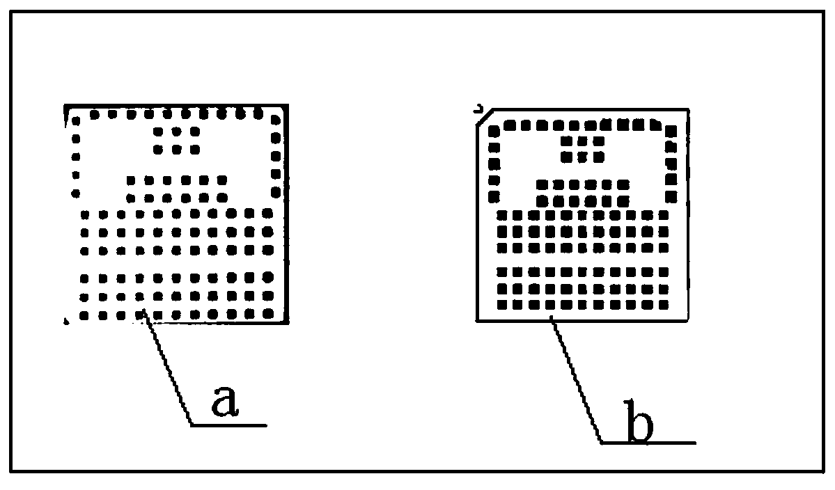
[0049] The chip-level steel mesh 6 is a flat steel mesh, and the flat steel mesh is provided with openings 11 whose area is equal to the area of the substrate surface contact 13 of the chip 10. Flat steel mesh requires less raw materials, short production cycle, low production process difficulty, high solder paste printing...
PUM
| Property | Measurement | Unit |
|---|---|---|
| Thickness | aaaaa | aaaaa |
| Width | aaaaa | aaaaa |
Abstract
Description
Claims
Application Information
 - R&D
- Intellectual Property
- Life Sciences
- Materials
- Tech Scout
- Unparalleled Data Quality
- Higher Quality Content
- 60% Fewer Hallucinations
Browse by: Latest US Patents, China's latest patents, Technical Efficacy Thesaurus, Application Domain, Technology Topic, Popular Technical Reports.
© 2025 PatSnap. All rights reserved.Legal|Privacy policy|Modern Slavery Act Transparency Statement|Sitemap|About US| Contact US: help@patsnap.com