Wafer carrier detection method and inspection tool

A carrier and wafer technology, which is applied in the field of chip manufacturing auxiliary tools, can solve the problems of easy deviation in wafer carrier detection, achieve the effect of not easy to detect errors, improve detection efficiency, and detect and judge quickly

Active Publication Date: 2020-08-04
KONFOONG MATERIALS INTERNATIONAL CO LTD
View PDF10 Cites 0 Cited by
  • Summary
  • Abstract
  • Description
  • Claims
  • Application Information

AI Technical Summary

Problems solved by technology

[0006] The purpose of the present invention is to provide a detection method for a wafer carrier, which solves the problem that the detection of wafer carriers in the prior art is prone to deviation by means of mounting detection

Method used


Image

  • Wafer carrier detection method and inspection tool
  • Wafer carrier detection method and inspection tool
  • Wafer carrier detection method and inspection tool

Examples


Embodiment 1

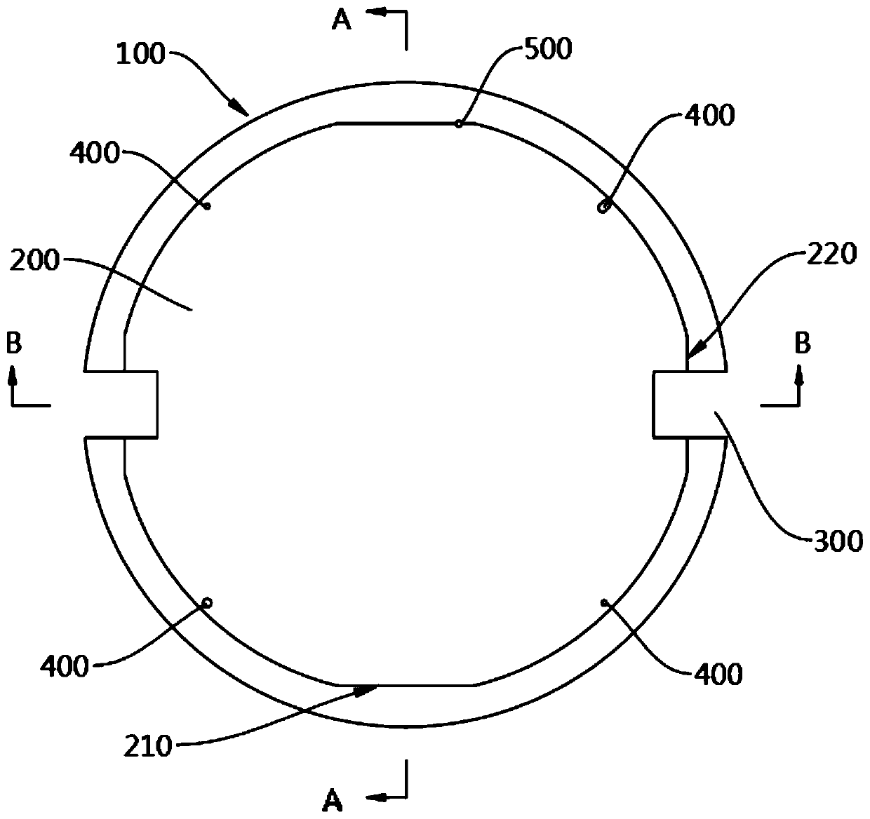
[0038] attached figure 1 It is a schematic diagram of the structure of wafer carrier 000; attached figure 2 is a schematic diagram of the three-dimensional structure of the inspection tool; Figure 3-6 It is a schematic diagram of the structure of the inspection tool under different viewing angles; Figure 7 , 8 It is a structural schematic diagram of the mounting device 600 under different viewing angles.

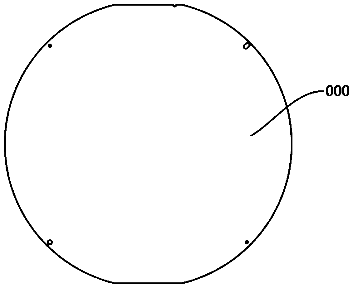
[0039] Please refer to attached figure 1 , the wafer carrier is roughly circular, and the edge is partially linear. There are four through holes on the wafer carrier 000, and an open half-hole is formed on the linear portion of the edge.

[0040] A wafer carrier 000 inspection tool is used for detecting the shape and size of the external structure of the wafer carrier, and for detecting the position and size of through holes and half holes on the wafer carrier.

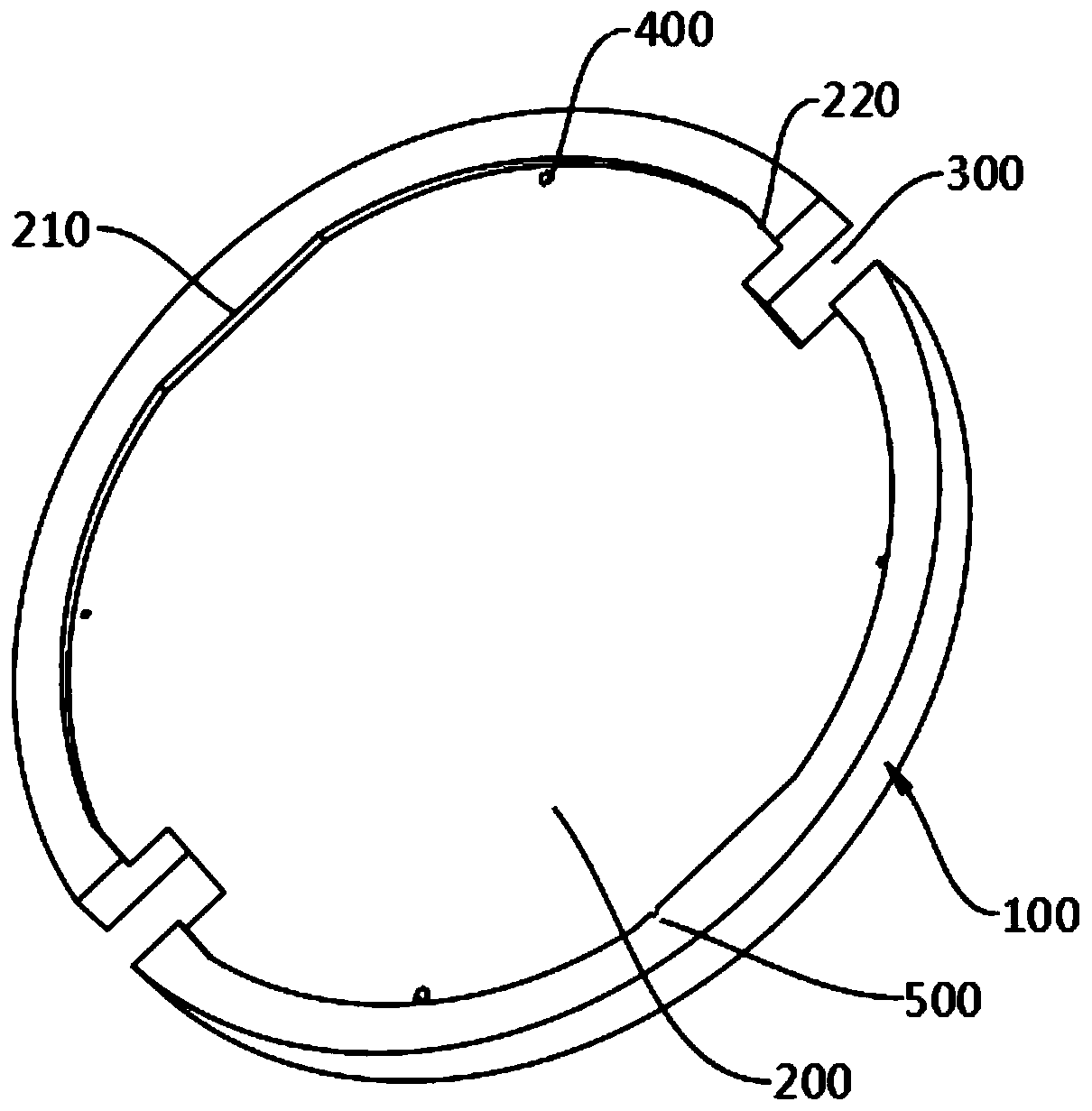
[0041] Please refer to attached figure 2 As shown, the tester includes a tester body 100, and the cente...

Embodiment 2

[0056] In order to further improve the detection efficiency, on the basis of Embodiment 1, a mounting tool 600 for assembling the plug gauge 900 is also provided to simultaneously detect multiple through holes and open half holes on the same wafer carrier 000. The tool 600 can help to speed up the efficiency of batch testing.

[0057] Please refer to attached Figure 7 with 8 As shown, the above-mentioned mounting tool 600 is provided with a plurality of mounting holes 700 for assembling plug gauges 900 , and the plug gauges 900 can be inserted and fixed in the mounting holes 700 .

[0058] An elastic ring is arranged in the installation hole 700, and the middle part of the elastic ring has a channel for clamping the plug gauge 900. The elastic ring can adapt to the plug gauge 900 of different specifications, and it is convenient to replace the plug gauge 900 of different specifications as required.

[0059] Please refer to attached Figure 7 with 8 As shown, in order to f...


PUM


Abstract

The invention relates to a chip manufacturing auxiliary tool, in particular to a wafer carrier detection method and a detection tool. The detection tool comprises a body, wherein a mounting groove used for mounting a wafer carrier is formed in the center of the body; a detection hole is formed in the mounting groove, and the detection hole corresponds to a through hole in the wafer carrier; and the size of the detection hole is larger than that of the through hole in the wafer carrier. The detection method requires the detection tool to be matched with a plug gauge, wherein the wafer carrier is placed in the detection tool with a standard containing cavity, and whether the edge of the wafer carrier is attached to the side wall of the standard containing cavity or not is observed; and thenthe plug gauge passes through the through hole in the wafer carrier, and is inserted into the corresponding detection hole in the standard containing cavity, and whether the plug gauge can pass through the through hole to be inserted into the detection hole or not is observed. By means of a breakthrough real equipment detection method, and by combination of the detection tool for implementation, whether the external structure and the hole position dimension of the wafer carrier are qualified or not can be seen clearly at the first glance, the detection error is not easy to occur, the judgmentis rapid, and the detection efficiency is high.

Description

technical field [0001] The invention relates to an auxiliary tool for chip fabrication, in particular to a detection method and a detection tool for a wafer carrier. Background technique [0002] Wafer is the carrier used in the production of integrated circuits, mostly referring to single crystal silicon wafers. In layman's terms, a wafer is composed of multiple chips. [0003] Generally, when producing chips, it is not produced one by one, but the wafers are produced first, and then the wafers are cut into chips one by one. [0004] The wafer carrier is the carrier placed under the wafer. The wafer carrier is installed on the detection machine position or the cutting machine position of the chip. The wafer carrier is provided with a through hole, which is used to adapt to the machine position. The through hole Whether the hole position and size of the wafer conform to the regulations, and whether the external structure of the wafer carrier itself conforms to the regulati...

Claims


Application Information

Patent Timeline
Patent Type & Authority Patents(China)
IPC IPC(8): G01B5/00
CPCG01B5/00
Inventor 姚力军潘杰王学泽陈文庆
Owner KONFOONG MATERIALS INTERNATIONAL CO LTD
Why Eureka
Try Eureka