A semiconductor device, a method of manufacturing the same, and an electronic device comprising the same

A semiconductor and device technology, applied in the field of acoustic semiconductor devices and their preparation, can solve problems such as leaking, poor low-frequency performance of devices, etc., and achieve the effect of improving low-frequency performance and high mechanical sensitivity

Inactive Publication Date: 2018-12-21
瑶芯微电子科技(上海)有限公司
View PDF6 Cites 1 Cited by
  • Summary
  • Abstract
  • Description
  • Claims
  • Application Information

AI Technical Summary

Problems solved by technology

The diaphragm 11 is fixed on the substrate through several anchor points. This structure can easily make the diaphragm have greater sensitivity, but it is not sealed, resulting in poor low-frequency performance of the device.

Method used


Image

  • A semiconductor device, a method of manufacturing the same, and an electronic device comprising the same
  • A semiconductor device, a method of manufacturing the same, and an electronic device comprising the same
  • A semiconductor device, a method of manufacturing the same, and an electronic device comprising the same

Examples


Embodiment Construction

[0035] In the following description, numerous specific details are given in order to provide a more thorough understanding of the present invention. It will be apparent, however, to one skilled in the art that the present invention may be practiced without one or more of these details. In other examples, some technical features known in the art are not described in order to avoid confusion with the present invention.

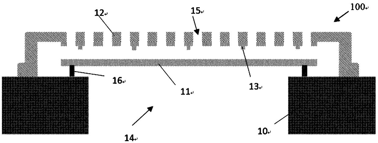
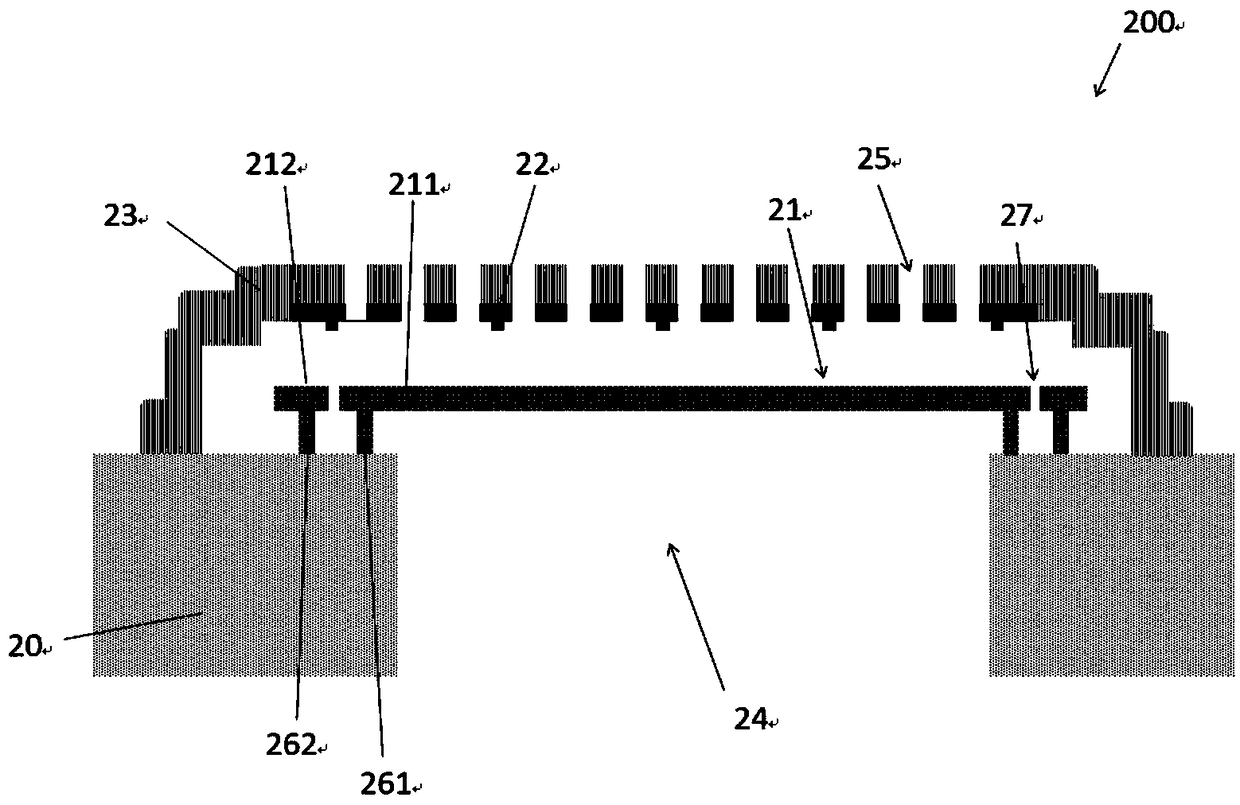
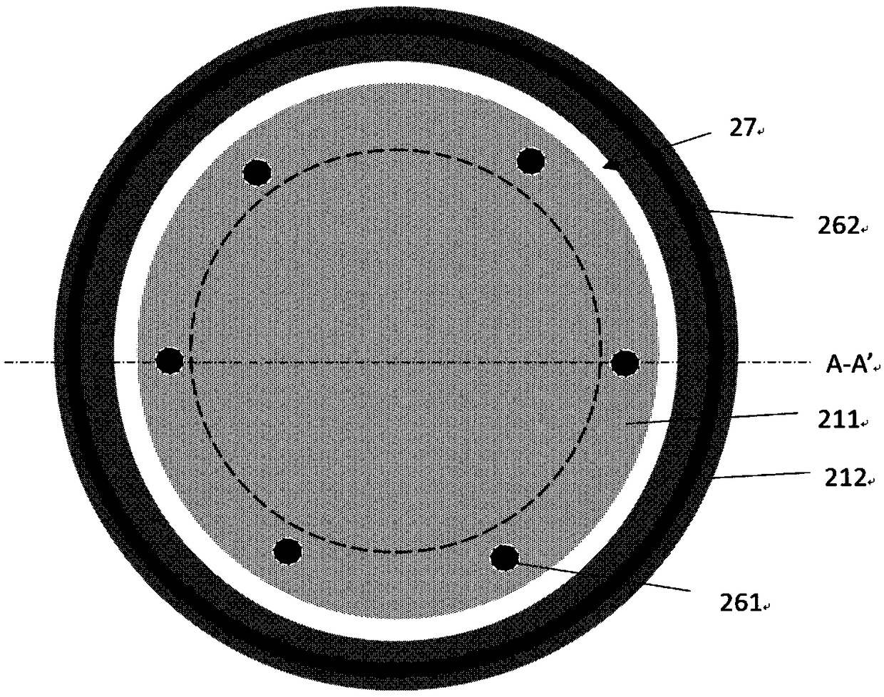
[0036] It should be understood that the invention can be embodied in different forms and should not be construed as limited to the embodiments set forth herein. Rather, these embodiments are provided so that this disclosure will be thorough and complete, and will fully convey the scope of the invention to those skilled in the art. In the drawings, the size and relative sizes of layers and regions may be exaggerated for clarity. Like reference numerals refer to like elements throughout.

[0037] It will be understood that when an element or layer is referred t...


PUM


Abstract

The invention discloses a semiconductor device, which is prepared on a substrate and comprises a diaphragm structure, a back plate structure and a back cavity. The diaphragm structure is characterizedin that the diaphragm structure comprises an intermediate diaphragm and a peripheral diaphragm, and a slit composed of the intermediate diaphragm and the peripheral diaphragm; The intermediate diaphragm is fixed on the substrate by a plurality of discrete anchors, and the peripheral diaphragm is fixed on the substrate by a membrane ring. The elatively sealed diaphragm can improve the low frequency performance of the device. The invention also discloses a preparation method of the semiconductor device and an electronic device comprising the semiconductor device.

Description

technical field [0001] Embodiments of the present invention relate to a semiconductor device, in particular to an acoustic semiconductor device and a manufacturing method thereof. Background technique [0002] In the field of semiconductors, a MEMS device is an acoustic transducer, which can feel the air vibration caused by the sound and make the movable electrode plate in the acoustic transducer do forced simple harmonic vibration, causing the change of the analog signal, and finally The sound signal is converted into an electrical signal. The acoustic transducer mainly includes the diaphragm, that is, the movable electrode plate; the back plate, that is, the fixed electrode plate; the back cavity structure, that is, the sound pressure signal enters the channel. [0003] figure 1 It is an existing acoustic transducer structure, wherein the diaphragm, the back plate (including the electrode layer and the insulating layer thereon), the through hole arranged on the back plat...

Claims


Application Information

Patent Timeline
Patent Type & Authority Applications(China)
IPC IPC(8): B81B7/02B81C1/00
CPCB81B7/02B81C1/00015
Inventor 吴冬冬
Owner 瑶芯微电子科技(上海)有限公司
Why Eureka
Try Eureka