
Absorption spectra of photoelectric devices based on ZnMgO/MgO/ZnO heterojunction materials

A technique for determining the absorption spectrum, which is applied in the production of quantum cascade lasers, the determination of the absorption spectrum of photoelectric devices, and the field of near-infrared photodetectors, can solve the problems of unfavorable working range accuracy, waste of financial and material resources, and inability to measure. Achieve the effects of improving performance, saving financial and material resources, and high precision

Active Publication Date: 2018-12-18
XIDIAN UNIV
View PDF4 Cites 2 Cited by
  • Summary
  • Abstract
  • Description
  • Claims
  • Application Information

AI Technical Summary

Problems solved by technology

However, these methods can only test and analyze the samples after the device preparation is basically completed, and cannot measure the absorption spectrum in the device simulation stage, so there is a more accurate prediction of the device absorption spectrum
It is not conducive to the determination of the working range and the improvement of accuracy in the device manufacturing process, and also wastes financial and material resources to a certain extent.

Method used


Image

  • Absorption spectra of photoelectric devices based on ZnMgO/MgO/ZnO heterojunction materials
  • Absorption spectra of photoelectric devices based on ZnMgO/MgO/ZnO heterojunction materials
  • Absorption spectra of photoelectric devices based on ZnMgO/MgO/ZnO heterojunction materials

Examples


Embodiment Construction

[0035] In order to make the purpose, technical solution and advantages of the present invention more clear, the following will further describe in detail in conjunction with the accompanying drawings and specific embodiments.

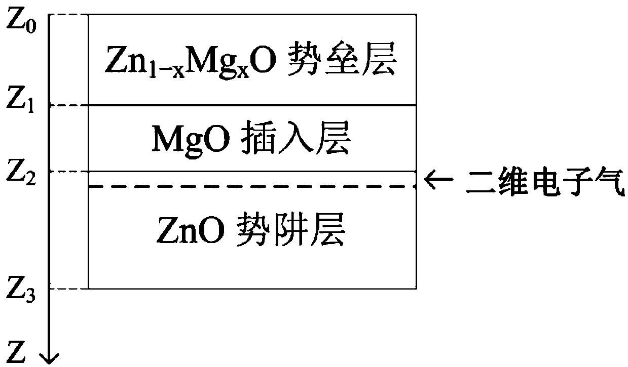
[0036] refer to figure 1 , the present invention, the photoelectric device absorption spectrum determination method based on ZnMgO / MgO / ZnO heterojunction material, its realization steps are as follows:

[0037] Step 1, setting the parameters of the ZnMgO / MgO / ZnO heterojunction.

[0038] 1.1) According to Zn 1-x Mg x The structure of the O / MgO / ZnO heterojunction sets the structural parameters of the heterojunction, which include the ZnMgO layer thickness d 1 , MgO layer thickness d 2 , ZnO layer thickness d 3 and Mg component x;

[0039] Zn in this example 1-x Mg x Zn in the structure of O / MgO / ZnO heterojunction 1-x Mg x The O material has a hexagonal wurtzite structure, the ZnO layer is selected as the substrate, the MgO layer is used as the i...


PUM


Abstract

The invention discloses a method for determining the absorption spectrum of an optoelectronic device based on a ZnMgO / MgO / ZnO heterojunction material, which mainly solves the problem that the existingoptoelectronic device cannot test the absorption spectrum before preparation. The method comprises the following steps: 1) setting parameters of the ZnMgO / MgO / ZnO heterojunction, sequentially calculating piezoelectric polarization intensity, polarization charge surface density, built-in electric field and conduction band order of the system in the heterojunction; 2) Simultaneous calculation of Fermi energy level, electron concentration and ionization impurity concentration, electron wave function and quantum energy level of the heterojunction; 3) calculating that optical absorption coefficient of the intersubband transition; 4) according to 1)-3), the optical absorption coefficients of intersubband transitions are calculated for different Mg compositions, different thickness of well layerand barrier layer, and the absorption spectra are obtained by fitting the parameters and formulas. The invention can determine the working band of the device before manufacturing the device, and canbe used for designing the photoelectric device based on the ZnMgO / MgO / ZnO heterojunction material.

Description

technical field [0001] The invention belongs to the technical field of microelectronics, and in particular relates to a method for determining the absorption spectrum of a photoelectric device, which can be used in the manufacture of near-infrared photodetectors and quantum cascade lasers. Background technique [0002] In recent years, many optoelectronic devices have been widely used, such as photodetectors, optical receivers, and optical amplifiers. The core working principle of these devices involves the process of electrons absorbing photons when they transition from a low-energy level to a high-energy level. The absorption spectrum is an important means to describe the relationship between the intensity of electronic transitions and the energy of incident light. At present, the absorption spectrum of photoelectric devices is mainly measured by infrared spectrometer, visible light divider, and X-ray absorption spectrometer. However, these methods can only test and analy...

Claims


Application Information

Patent Timeline
IPC IPC(8): G06F19/00
Inventor 刘妍王平
Owner XIDIAN UNIV
Learn More