A layer allocation method applied to a three-dimensional integrated circuit

A technology of integrated circuits and distribution methods, applied in special data processing applications, electrical digital data processing, instruments, etc., can solve problems such as lack of physical location information, low quality of layout results, and difficulty in ensuring layer allocation results. The effect of protecting the solution space, meeting high precision requirements, and good line length results

Pending Publication Date: 2018-12-18
CHINA UNIV OF MINING & TECH (BEIJING)
View PDF6 Cites 7 Cited by
  • Summary
  • Abstract
  • Description
  • Claims
  • Application Information

AI Technical Summary

Problems solved by technology

However, the quality of the layout results obtained by the three-dimensional layout method in the prior art is not high, lacks the necessary physical location information, it is difficult to guarantee the result of layer allocation, and cannot meet the high-precision requirements of integrated circuits

Method used


Image

  • A layer allocation method applied to a three-dimensional integrated circuit
  • A layer allocation method applied to a three-dimensional integrated circuit
  • A layer allocation method applied to a three-dimensional integrated circuit

Examples


Embodiment Construction

[0018] The technical solutions in the embodiments of the present invention will be clearly and completely described below in conjunction with the accompanying drawings in the embodiments of the present invention. Obviously, the described embodiments are only some of the embodiments of the present invention, not all of them. Based on the embodiments of the present invention, all other embodiments obtained by persons of ordinary skill in the art without making creative efforts belong to the protection scope of the present invention.

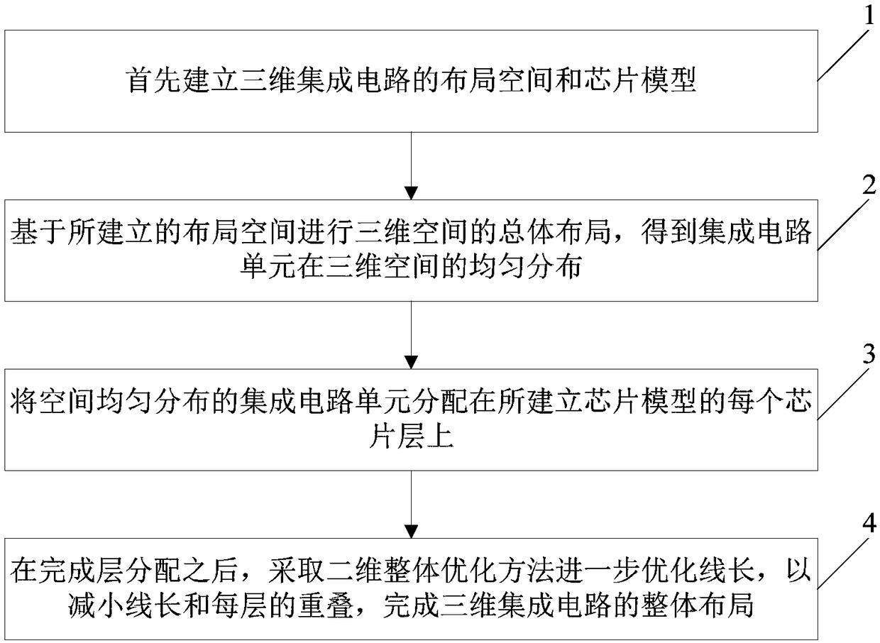
[0019] Embodiments of the present invention will be further described in detail below in conjunction with the accompanying drawings, as figure 1 Shown is a schematic flowchart of a layer allocation method applied to a three-dimensional integrated circuit provided by an embodiment of the present invention, and the method includes:

[0020] Step 1, first establish the layout space and chip model of the three-dimensional integrated circuit;

[0021] ...


PUM


Abstract

The invention discloses a layer allocation method applied to a three-dimensional integrated circuit. Firstly, a layout space and a chip model of the three-dimensional integrated circuit are established. Based on the established layout space, the overall layout of three-dimensional space is carried out, and the uniform distribution of integrated circuit cells in the three-dimensional space is obtained. Spatially uniformly distributed integrated circuit cells are distributed on each chip layer of the established chip model; after layer assignment, two-dimensional optimization method is adopted to further optimize the line length, so as to reduce the line length and the overlap of each layer and complete the overall layout of three-dimensional integrated circuits. The above method can inheritthe three-dimensional optimization results as far as possible and protect the solution space, so as to obtain better line length results, the number of TSVs and running time, and meet the high-precision requirements of integrated circuits.

Description

technical field [0001] The invention relates to the technical field of integrated circuits, in particular to a layer allocation method applied to three-dimensional integrated circuits. Background technique [0002] With the rapid development of the information age, the hardware part of the computer has become a bottleneck for the rapid development of the information society. Although the integration of chips is getting higher and higher, it is also due to the sharp increase in the integration that has brought about the development of the chip design field. important problem. In the past ten years, the chip manufacturing process has also developed from 130nm level in 2002 to the current 22nm level. The continuous development of integrated circuit manufacturing technology has also brought many new problems. The reduction of the interconnection line width in the chip And the increase of the length of the interconnection line leads to the continuous increase of the delay on the...

Claims


Application Information

Patent Timeline
Patent Type & Authority Applications(China)
IPC IPC(8): G06F17/50
CPCG06F30/392G06F30/367
Inventor 高文超
Owner CHINA UNIV OF MINING & TECH (BEIJING)
Why Eureka
Try Eureka