Ferroelectric thin film transistor, organic light emitting array substrate driving circuit and display device

A ferroelectric thin film and transistor technology, applied in the direction of transistors, circuits, electrical components, etc., can solve the problems of complex driving circuits, and achieve the effects of simplifying the driving circuit, improving display performance, good retention and durability.

Active Publication Date: 2018-12-14
UNIV OF SCI & TECH OF CHINA
View PDF3 Cites 2 Cited by
  • Summary
  • Abstract
  • Description
  • Claims
  • Application Information

AI Technical Summary

Problems solved by technology

It can be found that in the entire display area, each sub-pixel requires at least two thin film transistors and a storage capacitor for driving, which makes the driving circuit more complicated

Method used


Image

  • Ferroelectric thin film transistor, organic light emitting array substrate driving circuit and display device
  • Ferroelectric thin film transistor, organic light emitting array substrate driving circuit and display device
  • Ferroelectric thin film transistor, organic light emitting array substrate driving circuit and display device

Examples


Embodiment Construction

[0039] The following will clearly and completely describe the technical solutions in the embodiments of the present invention with reference to the accompanying drawings in the embodiments of the present invention. Obviously, the described embodiments are only some, not all, embodiments of the present invention. Based on the embodiments of the present invention, all other embodiments obtained by persons of ordinary skill in the art without making creative efforts belong to the protection scope of the present invention.

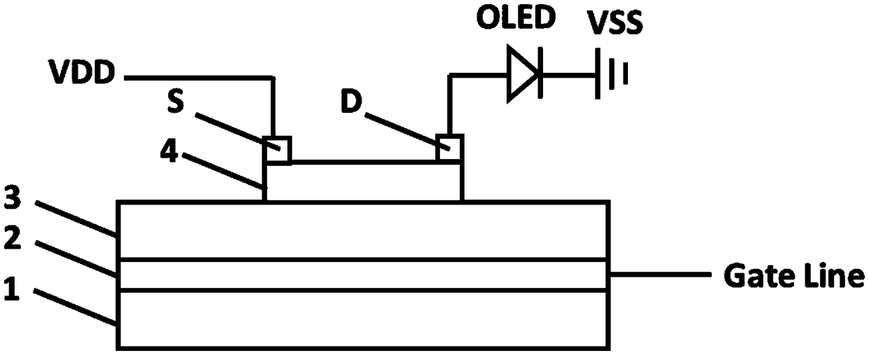
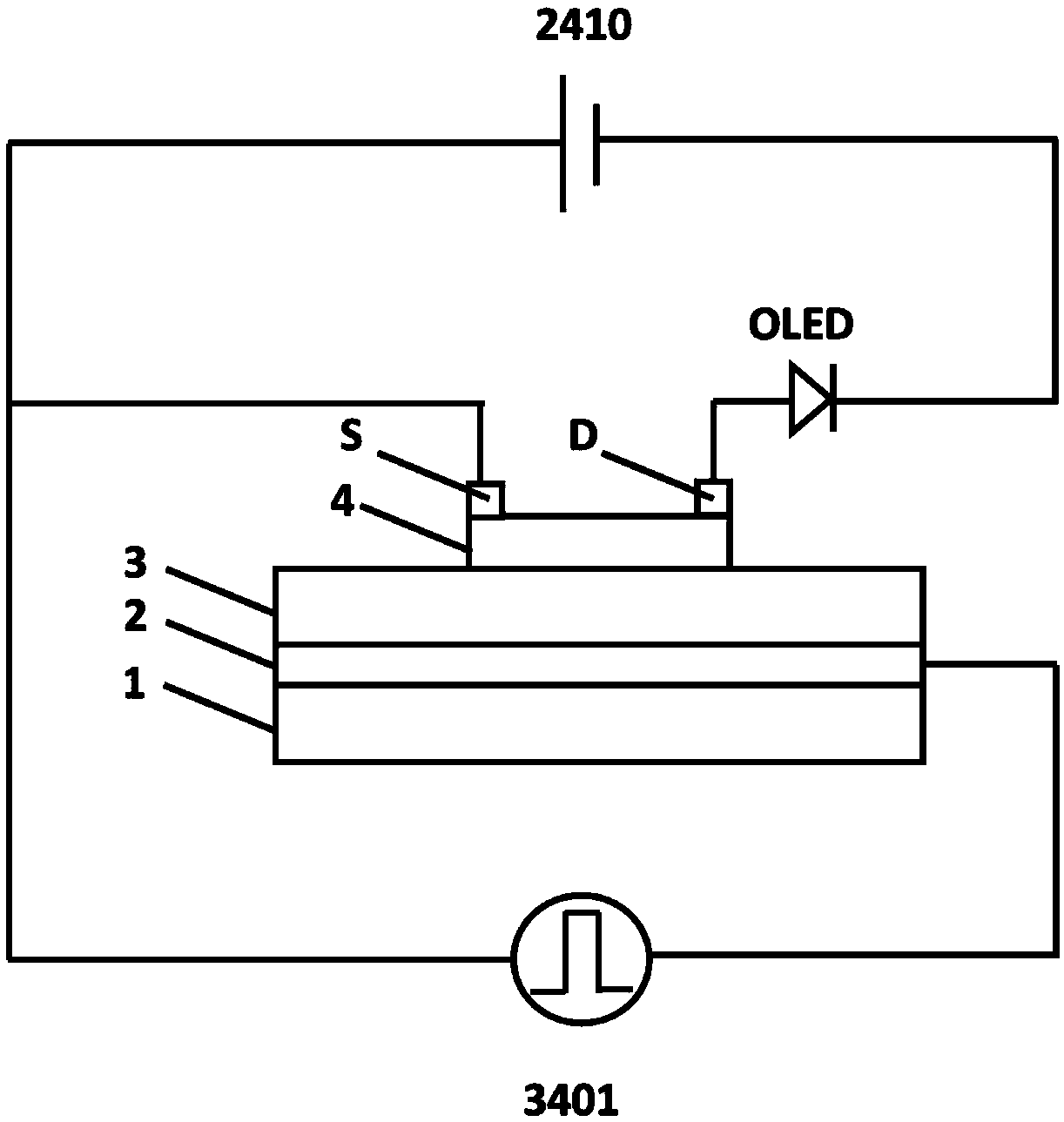
[0040] Aiming at the problem in the prior art that each pixel unit requires at least two thin film transistors and a storage capacitor to drive, which makes the structure of the driving circuit of the pixel unit complicated, this application discloses a ferroelectric thin film transistor, an organic light emitting array substrate drive circuit and display device.

[0041] figure 2 For a schematic structural diagram of an OLED pixel drive circuit based on a s...


PUM


Abstract

The invention provides a ferroelectric thin film transistor, an organic light emitting array substrate driving circuit and a display device. The ferroelectric thin film transistor comprises a substrate; a bottom electrode layer arranged on the substrate; a ferroelectric layer disposed on one side of the bottom electrode layer back to the substrate, the ferroelectric layer being made of a materialhaving nonvolatile ferroelectric polarization; a semiconductor channel layer disposed on one side of the ferroelectric layer back to the substrate; and a source electrode and a drain electrode arranged on one side of the semiconductor channel layer back to the substrate. The drain electrode is used for being connected with an input end of a light emitting element; the source electrode is used forbeing connected with a power supply signal line; the bottom electrode layer is used for being connected with a control signal line; and a driving circuit is simple. The polarization state of the ferroelectric layer is regulated by applying voltage to the bottom electrode layer, and then the concentration and resistance of carriers in the semiconductor channel layer are regulated through the polarization state of the ferroelectric layer to change the magnitude of the current flowing through an OLED, so that the continuous modulation of the OLED series voltage division and the OLED display withdifferent gray scales are realized, and a control mode is simple.

Description

technical field [0001] The invention relates to the technical field of semiconductors and electronic circuits, in particular to a nonvolatile ferroelectric regulated ferroelectric thin film transistor, an organic light emitting array substrate drive circuit and a display device. Background technique [0002] Organic Light-Emitting Display (OLED) has been widely valued due to its characteristics such as self-illumination, wide viewing angle, high color gamut, high contrast ratio, and low power consumption. [0003] OLED display devices can be classified into two types according to their driving methods: Passive Matrix OLED (PMOLED) and Active Matrix OLED (AMOLED). Among them, AMOLED is an active display type, and is usually used as a high-definition display device. AMOLEDs are current driven devices. When a current flows through the organic light emitting diode, the diode emits light, and the brightness of the light is determined by the magnitude of the flowing current. ...

Claims


Application Information

Patent Timeline
Patent Type & Authority Applications(China)
IPC IPC(8): H01L29/78H01L29/786G09G3/3233
CPCG09G3/3233H01L29/78606H01L29/78391
Inventor 刘川川苏同上殷月伟李晓光
Owner UNIV OF SCI & TECH OF CHINA
Why Eureka
Try Eureka