Strong-absorption optothermal detector and preparation method thereof
A photothermal detection and detector technology, applied in the field of detectors, can solve the problems of weak light absorption capacity of photothermal detectors, and achieve the effects of improving photothermal detection accuracy, sensitivity and absorption capacity.
- Summary
- Abstract
- Description
- Claims
- Application Information
AI Technical Summary
Problems solved by technology
Method used
Image
Examples
Embodiment 1
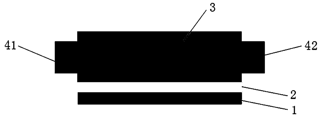
[0025] Such as figure 1 Shown is a strong absorption photothermal detector in this embodiment, which is composed of a base layer 1, a photothermal detection structure 3, a first electrode 41 and a second electrode 42, and the photothermal detection structure 3 covers the base layer 1. The first electrode 41 and the second electrode 42 are respectively connected to two sides of the photothermal detector.
[0026] Specifically: the base layer 1 of this embodiment is preferably ITO glass, which has excellent photoelectric properties, strong electrical conductivity and high light transmittance. When the incident light hits the photothermal detection structure 3, the light signal is converted into an electrical signal, and then the external circuit is connected through the first electrode 41 and the second electrode 42, and the telecommunication is output to the display device. purpose of heat detection.
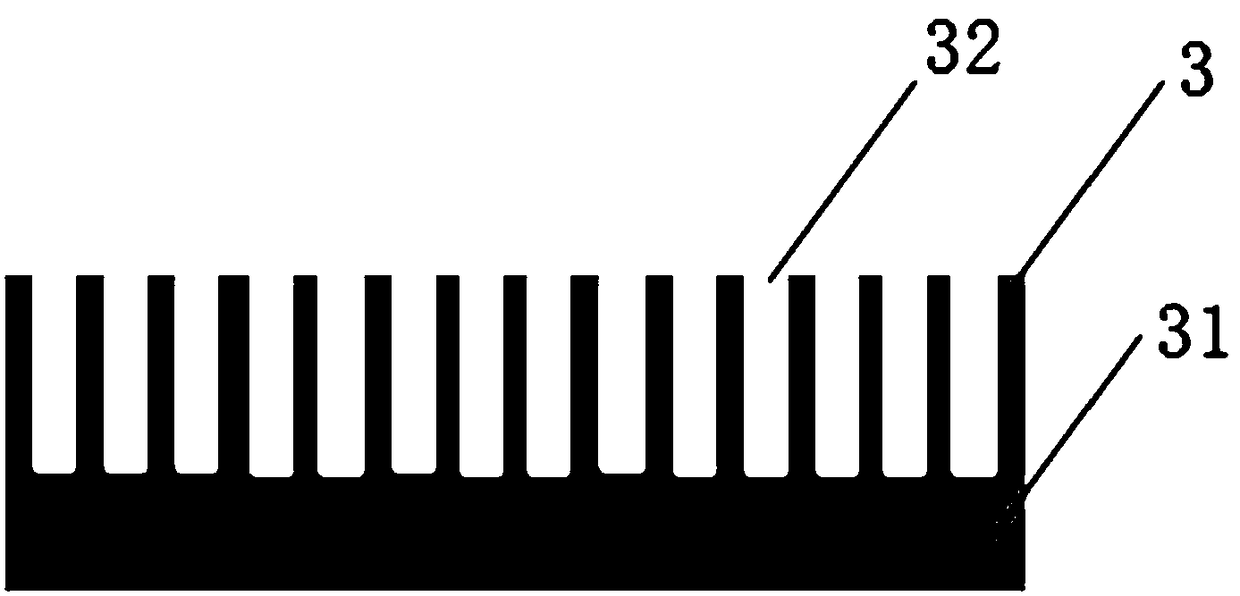
[0027] In this embodiment, the photothermal detection structure 3 includes...
Embodiment 2
[0035] Based on the strong absorption photothermal detector disclosed in Example 1, this embodiment discloses a preparation method of a strong absorption photothermal detector, including the following steps:
[0036] Step 1, preparing the base layer 1, and evaporating silicon dioxide on the base layer 1 by electron beam evaporation to form a dielectric layer 2;
[0037] Step 2, vapor-depositing silicon germanium on the dielectric layer 2 formed in step 1 by physical vapor deposition to form heat sensitive lines 31;
[0038] Step 3, using a pattern generator to design the shape of the microhole 32, and then using focused ion beam technology to etch the microhole 32 on the thermally sensitive line 31 formed in step 2;
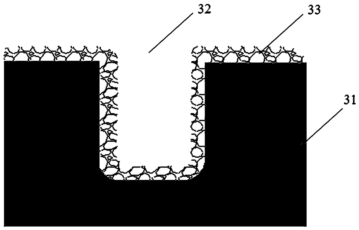
[0039] Step 4. Evaporate noble metal particles on the heat-sensitive wire 31 containing micropores 32 prepared in step 3 by electron beam evaporation, and form a layer of noble metal particle layer 33 on the surface of the heat-sensitive wire 31 and the surface o...
PUM
| Property | Measurement | Unit |
|---|---|---|
| Thickness | aaaaa | aaaaa |
| Depth | aaaaa | aaaaa |
| Diameter | aaaaa | aaaaa |
Abstract
Description
Claims
Application Information
 - R&D
- Intellectual Property
- Life Sciences
- Materials
- Tech Scout
- Unparalleled Data Quality
- Higher Quality Content
- 60% Fewer Hallucinations
Browse by: Latest US Patents, China's latest patents, Technical Efficacy Thesaurus, Application Domain, Technology Topic, Popular Technical Reports.
© 2025 PatSnap. All rights reserved.Legal|Privacy policy|Modern Slavery Act Transparency Statement|Sitemap|About US| Contact US: help@patsnap.com


